
당신은 주제를 찾고 있습니까 “testout network pro 13.4.8 – 13.4.5 Packet Tracer – Troubleshoot WLAN Issues“? 다음 카테고리의 웹사이트 https://ppa.charoenmotorcycles.com 에서 귀하의 모든 질문에 답변해 드립니다: ppa.charoenmotorcycles.com/blog. 바로 아래에서 답을 찾을 수 있습니다. 작성자 Tech Acad 이(가) 작성한 기사에는 조회수 23,185회 및 좋아요 348개 개의 좋아요가 있습니다.
testout network pro 13.4.8 주제에 대한 동영상 보기
여기에서 이 주제에 대한 비디오를 시청하십시오. 주의 깊게 살펴보고 읽고 있는 내용에 대한 피드백을 제공하세요!
d여기에서 13.4.5 Packet Tracer – Troubleshoot WLAN Issues – testout network pro 13.4.8 주제에 대한 세부정보를 참조하세요
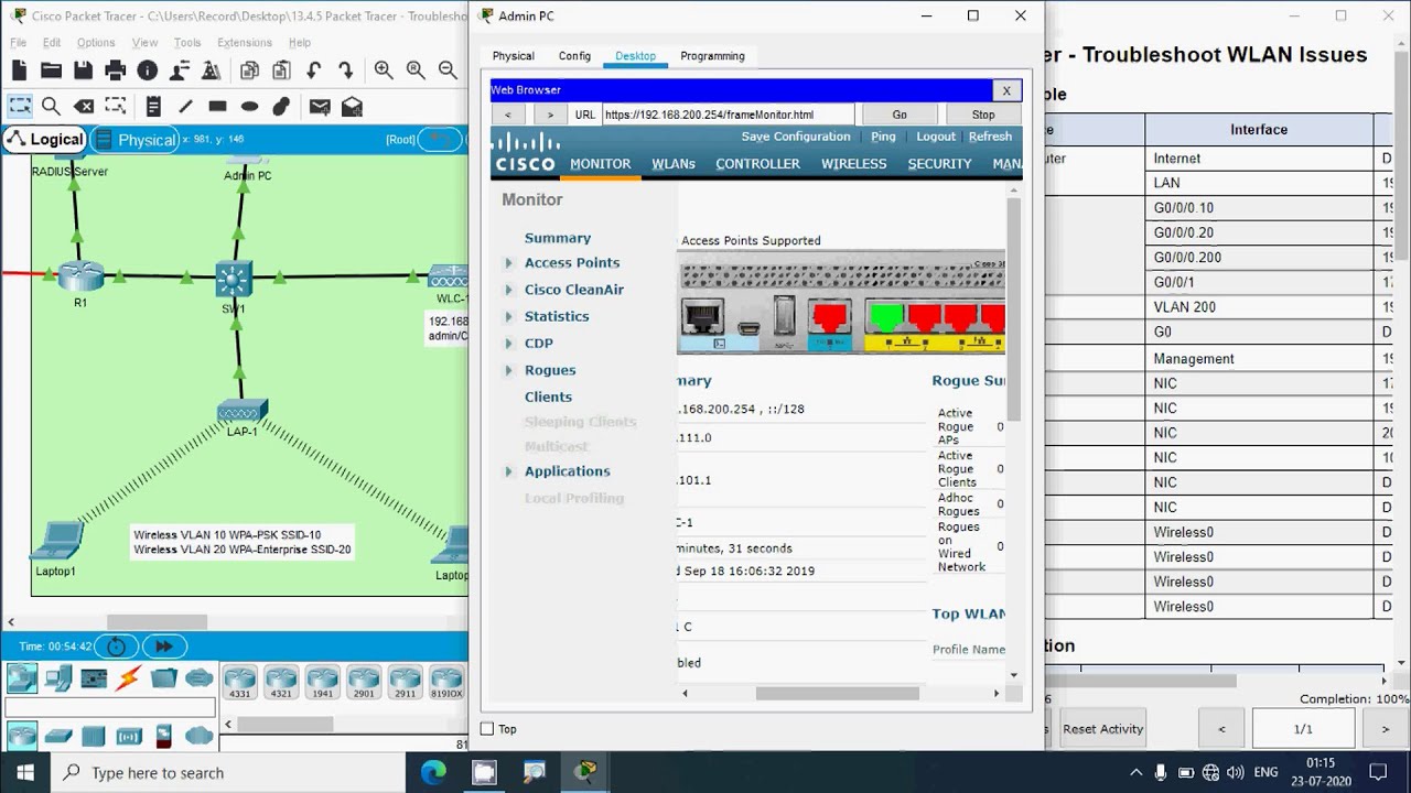
13.4.5 Packet Tracer – Troubleshoot WLAN Issues
CCNAv7 – Switching, Routing, and Wireless Essentials
Visit our Website to contact us: http://www.techacadhelp.com
Follow us on Facebook: https://www.facebook.com/techacad4u
testout network pro 13.4.8 주제에 대한 자세한 내용은 여기를 참조하세요.
TestOut Network Pro – COURSE OUTLINE
0.1.1 Network Pro Introduction (3:35). 0.2 Use the Simulator … TestOut Network Pro Outline – English 5.0.x … 13.4.8 Practice Questions.
Source: www.digiterati.com
Date Published: 8/15/2021
View: 3694
Testout PC Pro Course Outline – Tech Vision Resources
PC Pro Outline … 1.1.1 PC Pro and A+ Certification (9:03) … 13.4.7 Network Troubleshooting Facts 2; 13.4.8 Fix a Network Connection 1 …
Source: database.techvisionresources.com
Date Published: 9/22/2022
View: 4878
User’s Guide – Fujitsu
Windows® 7 Professional … 13.4.8 Encapsulation. … If the specified computer-name does not exist on the network, or if Windows(x64) is not running on the …
Source: software.fujitsu.com
Date Published: 10/30/2021
View: 9765
Full text of “Philips: pm3065 pm3067” – Internet Archive
4 .3 MIL-STD-810 method 516, pro- ced, V MIL-T-28800C par. … sensitivity MTB Sine-wave 13.4.8 80 mV – 10 kHz R4108 MTB gain 1 ms time marker 1 ms 13.4.9 …
Source: archive.org
Date Published: 12/26/2022
View: 1723
d2l-en.pdf – Dive into Deep Learning
Recurrent Neural Network Implementation from Scratch . … 13.4.8 Summary . … we might enumerate all the common events that our pro-.
Source: d2l.ai
Date Published: 8/9/2021
View: 9899
주제와 관련된 이미지 testout network pro 13.4.8
주제와 관련된 더 많은 사진을 참조하십시오 13.4.5 Packet Tracer – Troubleshoot WLAN Issues. 댓글에서 더 많은 관련 이미지를 보거나 필요한 경우 더 많은 관련 기사를 볼 수 있습니다.
주제에 대한 기사 평가 testout network pro 13.4.8
- Author: Tech Acad
- Views: 조회수 23,185회
- Likes: 좋아요 348개
- Date Published: 2020. 7. 25.
- Video Url link: https://www.youtube.com/watch?v=kbjc0_axy0U
Full text of “Philips: pm3065 pm3067”
Full text of “Philips: pm3065 pm3067”
100 MHz Dual Time Base Oscilloscope PM3065 PM3067 Service Manual 4822 872 05323 880229/1 Industrial & Electro-acoustic Systems PHILIPS 100 MHz Dual Time Base Oscilloscope PM3065 PM3067 Service Manual 4822 872 05323 880229/1 WARNING: These servicing instructions are for use by qualified pe To reduce the risk of electric shock do not perform any then that specified in the Operating Instructions unless qualified to do so. rsonnel only, servicing other you are fully 2 IMPORTANT NOTE: © R.V. : In correspondence concerning this instrument, please quote the type number and serial number as given on the type plate. The design of this instrument is subject to continuous development and improvement. Consequently, this instrument may incorporate minor changes in detail from the information contained in this manual. PHILIPS GLOEILAMPENFABRIEKEN-EINDHOVEN-THE NETHERLANDS- 19 8 8 PAINTED IN THE NETHERLANDS 3 CONTENTS Page 1. SAFETY INSTRUCTIONS 1-1 1.1 Introduction 1-1 1.2 Safety precautions 1-1 1.3 Caution and warning statements 1-1 1.4 Symbols 1-1 1.5 Impaired safety-protection 1-2 1.6 General clauses 1-2 2. CHARACTERISTICS 2-1 2.1 Display 2-3 2.2 Vertical deflections or Y axis 2-4 2.2.1 Channels A and B 2-4 2.2.2 Triggerview 2-5 2.3 Horizontal deflection or X axis 2-6 2.3.1 Main Time Base (MTB) 2-6 2.3.2 Delayed Time Base (DTB) 2-6 2.3.3 X-deflection 2-7 2.3.4 EXT input 2-7 2.4 Triggering 2-8 2.4.1 MTB triggering 2-8 2.4.2 DTB triggering 2-9 2.5 Power supply 2-9 2.6 Auxiliary inputs or outputs 2-10 2.7 Environmental characteristics 2-10 2.8 Safety 2-12 3. INTRODUCTION TO CIRCUIT DESCRIPTION AND BLOCK DIAGRAM DESCRIPTION 3-1 3.1 Introduction to circuit description 3-1 3.2 Block diagram description 3-12 3.2.1 Introduction 3-12 3.2.2 Control unit 3-12 3.2.3 Attenuator unit 3-12 3.2.4 Pre-amplifier unit 3-12 3.2.5 Time-base unit 3-14 3.2.6 XYZ unit 3-14 3.2.7 Power supply unit 3-15 4 4. ATTENUATOR UNIT (Al) 4.1 Vertical attenuators 4.2 External input ^“2 5. PRE-AMPLIFIER UNIT (A2) 5-1 5.1 Vertical pre-amplifier 5-1 5.2 MTB trigger pre-amplifier 5-2 5.3 DTB trigger pre-amplifier 5-3 5.4 Pre-amplifier control 5-4 6. XYZ-AMPLIFIER UNIT (A3) 6-1 6.1 Introduction 6-1 6.2 Final vertical (Y) amplifier 6-1 6.3 Final horizontal X) amplifier 6-1 6.4 Final blanking (Z) amplifier and CRT 6-2 7. TIME-BASE UNIT (A4) 7-1 7.1 Trigger amplifier 7-1 7.2 Timing circuit 7-2 7.3 Sweep generators 7-4 7.4 X DEFL amplifier, and display mode switch 7-6 7.5 Z-amplifier 7-7 7.6 Timing diagrams 7-8 8. CRT CONTROL UNIT (A5) 6-1 9. POWER SUPPLY UNIT (A6) 9-1 9.1 Input circuit 9-1 9.2 Converter circuit 9-1 9.3 Secondary output rectifiers 9-2 9.4 HT supply 9-3 9.5 Calibrator 9-3 5 10. FRONT UNIT (A7-A8) 10-1 10.1 10 . 1.1 10.1.2 10.1.3 10.1.4 10.1.5 10.1.6 10.1.7 10.1.8 Microcomputer control circuit Introduction to MAB8052 microcomputer Characteristics of the I’^C bus 2 I C structure Microcomputer MAB8052 I^C decoding Status input Probe indicator C-Bus decoder 10-1 10-1 10-1 10-2 10-3 10-4 10-4 10-5 10-5 10.2 LCD display circuit 10-5 10.3 Front-panel controls 10-5 1 1 . PERFORMANCE CHECK 11-1 11.1 General information 11-1 11.2 Preliminary settings 11-2 11.3 Recommended test equipment 11-2 11.4 11.4.1 11.4.2 11.4.3 11.4.4 11.4.5 11.4.6 11.4.7 11.4.8 Checking procedure Power supply Display Vertical deflection or Y-axis . Trigger view Horizontal deflection or X-axis MTB triggering DT6 triggering Auxiliary inputs and outputs . . 11-3 11-3 11-3 11-4 11-10 11-13 11-18 11-21 11-22 12. DISMANTLING THE INSTRUMENT 12.1 General information 12.2 Removing the top and bottom covers 12.3 Access to parts for the checking and adjusting procedures 12-1 12-1 12-1 12-1 13. CHECKING AND ADJUSTING 13.1 13.2 13-1 13-1 13-6 13.3 General information Recommended test and calibration equipment Survey of adjusting elements 13-7 6 13.4 Checking and adjusting procedure 13-9 13.4.1 Preparation 13-9 13.4.2 Power supply adjustment 13-9 13.4.3 CRT display adjustment 13-9 13.4.4 Square-wave response attenuator • . • • 13-10 13.4.5 Adjustment of vertical sensitivities 13-11 13.4.6 Adjustment of horizontal sensitivity 13-11 13.4.7 Offset adjustments – 13-12 13.4.8 Adjustment of trigger sensitivity 13-12 13.4.9 Adjustment of the MTB sweep times 13-12 13.4.10 Adjustment of the DTB sweep times 13-13 13.4.11 Adjustment of xlO sweep times 13-13 13.4.12 Adjustment of delay time multiplier 13-13 13.4.13 Square-wave response 13-14 13.4.14 Checking the AUTO SET function 13-15 14. CORRECTIVE MAINTENANCE 14-1 14.1 Replacements 14-1 14.1.1 Standard parts 14-1 14.1.2 Special parts 14-1 14.1.3 Transistors and integrated circuits 14-1 14.1.4 Static-sensitive components 14-2 14.1.5 Handling MOS devices 14-2 14.1.6 Soldering and desoldering of surface mounted devices on unit 8 14-3 14.2 Removing the units and mechanical parts 14-5 14.2.1 Attenuator unit (Al) 14-5 14.2.2 Pre-amplifier unit (A2) 14-5 14.2.3 XYZ-amplif ier unit (A3) 14-5 14.2.4 Time-base unit (A4) 14-6 14.2.5 CRT control unit (A5) 14-6 14.2.6 Power supply unit (A6) 14-6 14.2.7 Front unit (A7) and LCD unit (A8) 14-8 14.2.8 Removing the delay line cable 14-9 14.2 . 9 Replacement of CRT 14-9 14.3 Soldering techniques 14-10 14.4 Instrument repacking 14-10 14.5 Trouble shooting 14-11 14.5.1 Introduction 14-11 14.5.2 Trouble-shooting techniques 14-11 14.5.3 Power-up routine 14-12 14.5.4 Trouble-shooting the power supply 14-12 14.5.5 P.c.b. interconnections 14-13 14.6 Special tools 14-13 14.6.1 Trimming Kit SBC 317 14-13 14.6.2 P.c.b. snapper 14-18 14.7 Recalibration after repair 14-18 7 15. SAFETY INSPECTION AND TEST AFTER REPAIR AND MAINTENANCE IN THE PRIMARY CIRCUIT 15-1 15.1 General directives 15-1 15.2 Safety components 15-1 15.3 Checking the protective earth connection 15-1 15.4 Checking the insulation resistance 15-1 15.5 Checking the leakage current 15-1 15.6 Voltage test 15-2 16. PARTS LIST 16-1 16.1 Mechanical parts 16-1 16.2 Units 16-6 16.3 Cables and connectors 16-7 16.3.1 Flatcables and connectors 16-7 16.3.2 P.c.b. -connectors 16-7 16.3.3 Miscellaneous cables 16-7 16.4 Electrical parts 16-8 16.4.1 Capacitors 16-8 16.4.2 Resistors 16-11 16.4.3 Coils 16-16 16.4.4 Semi-conductors 16-17 16.4.5 Integrated circuits 16-19 16.4.6 Cathode ray tube 16-19 16.4.7 Miscellaneous 16-19 17. OPTIONS 17-1 17.1 MTB gate 17-1 17.2 DTB gate 17-1 17.3 MTB sweep 17-2 17.4 Parts list 17-2 8 LIST OF FIGURES Page Figure 2.1 Dimensions 2-2 Figure 2.2 Maximum input voltage versus frequency 2-3 Figure 3.1 Block diagram ^*7 Figure 4.1 Table of attenuator settings 4-1 Figure 4.2 Attenuator unit p.c.b. 4-3 Figure 4.3 Circuit diagram of attenuator, ch. A 1 4-5 Figure 4.4 Circuit diagram of attenuator, ch. A 2 4-8 Figure 4.5 Attenuator unit p.c.b. ^”9 Figure 4.6 Circuit diagram of attenuator, ch. B 1 4-11 Figure 4.7 Circuit diagram of attenuator, ch. B 2 4-12 Figure 4.8 Attenuator unit p.c.b. 4-14 Figure 4.9 Circuit diagram of attenuator, EXT 4-16 Figure 5.1 The four stages of the vertical pre-aplifier 5-1 Figure 5.2 Pre-amplifier unit p.c.b. 3-5 Figure 5.3 Circuit diagram of pre-amplifier, channel switch 5-7 Figure 5.4 Circuit diagram of pre-amplifier, delay line driver 5-8 Figure 5.5 Pre-amplifier unit p.c.b. 5-10 Figure 5.6 Circuit diagram of pre-amplifier, MTB trigger switch 5-12 Figure 5.7 Circuit diagram of pre-amplifier, level circuit 5-13 Figure 5.8 Pre-amplifier unit p.c.b. 5-15 Figure 5.9 Circuit diagram of pre-amplifier, DTB trigger switch 5-17 Figure 5.10 Circuit diagram of pre-amplifier, logic control 5-18 Figure 5.11 Pre-amplifier unit p.c.b. 5-20 Figure 5.12 Circuit diagram of pre-amplifier, supply voltages 5-22 Figure 6.1 XYZ amplifier unit p.c.b. 6-3 Figure 6.2 Circuit diagram of XYZ amplifier, final Y amplifier 6-5 Figure 6.3 Circuit diagram of XYZ amplifier, final X amplifier 6-6 Figure 6.4 XYZ amplifier unit p.c.b. 6-8 Figure 6.5 Circuit diagram of XYZ amplifier, Z amplifier 6-10 Figure 6.6 Circuit diagram of XYZ amplifier, CRT circuit 6-12 Figure 7.1 D4103 configuration 7-2 Figure 7.2 Simplified diagram of the MTB 7-4 Figure 7.3 Z-logic for the different TB modes 7-7 Figure 7.4 Free-running MTB sweep-timing diagram 7-8 Figure 7.5 Triggered MTB-sweep with a delay sweep-timing diagram 7-8 Figure 7.6 Triggered MTB- and TDB-sweep-timing diagram 7-9 Figure 7.7 Time base unit p.c.b. 7-11 Figure 7.8 Circuit diagram of time base, trigger amplifier MTB and DTB 7-13 Figure 7.9 Circuit diagram of time base, MTB and DTB sweep circuits and final X DEFL amplifier 7-14 Figure 7.10 Time base unit p.c.b. 7-16 Figure 7.11 Circuit diagram of time base, X pre-amplifier and Z switch 7-18 Figure 8.1 Circuit diagram of CRT control 8-1 Figure 8.2 CRT control unit p.c.b. 8-1 Figure 9.1 Converter circuit 9-2 Figure 9.2 Timing diagram converter circuit 9-2 Figure 9.3 HT oscillator 9-3 Figure 9.4 Power supply unit p.c.b. 9-5 Figure 9.5 Circuit diagram of power supply 9-8 9 Figure 10.1 Bit transfer 10-1 Figure 10.2 Definition of start and stop conditions 10-2 Figure 10.3 I^C structure 10-2 Figure 10.4 Pinning of microcomputer MAB 8052 10-3 Figure 10.5 Front unit p.c.b. 10-6 Figure 10.6 Circuit diagram of front unit 10-8 Figure 10.7 LCD unit p.c.b. 10-9 Figure 10.8 Circuit diagram of LCD unit 10-10 Figure 11.1 SOFTSTART condition 11-2 Figure 12.1 Access to all parts for checking and adjusting 12-2 Figure 13.1 Adjusting elements 13-4 Figure 13.2 Square-wave response 13-14 Figure 14.1 Arrangement of working area for S.M.D. exchange and MOS device 14-3 Figure 14.2 Six clamping lips for XYZ-amplifier unit 14-6 Figure 14.3 Power supply unit outside the instrument 14-7 Figure 14.4 Measuring the front unit working condition 14-8 Figure 14.5 Removing the CRT 14-9 Figure 14.6 P.c.b. interconnections 14-15 Figure 14.7 Trimming tool kit 14-18 Figure 14.8 P.c.b. snapper 14-18 Figure 16.1 Exploded view 16-3 Figure 16.2 Rear view 16-5 Figure 16.3 Inside view showing the parts in the CRT compartment 16-5 Figure 16.4 View of the units 16-5 Figure 17.1 Circuit diagram of MTB gate, DTB gate and MTB sweep options 17-2 Figure 17.2 P.c.b. for MTB gate, DTB gate and MTB sweep 17-2 1-1 1. SAFETY INSTRUCTIONS Read these pages carefully before installation and use of the instrument . 1.1 INTRODUCTION The following clauses contain infomation, cautions and warnings which must be followed to ensure safe operation and to retain the instrument in a safe condition. Adjustment, maintenance and repair of the instrument shall be carried out only by qualified personnel. 1.2 SAFETY PRECAUTIONS For the correct and safe use of this instrument it is essential that both operating and servicing personnel follow generally-accepted safety procedures in addition to the safety precautions specified in this manual . Specific warning and caution statements, where they apply, will be found throughout the manual. Where necessary, the warning and caution statements and/or s}nnbols are marked on the apparatus . 1.3 CAUTION AND WARNING STATEMENTS CAUTION: is used to indicate correct operating or maintentance procedures in order to prevent damage to or destruction of the equipment or other property. WARNING: calls attention to a potential danger that requires correct procedures or pracites in order to prevent personal injury. 1.4 SYMBOLS ^ High voltage ^ 1000 V (red) A Live part (black/yellow) A Read the operating instructions Protective earth ( grounding ) terminal (black) 1-2 1 . 5 IMPAIRED SAFETY-PROTECTION Whenever it is likely that safety-protection has been impaired, the instrument must be made inoperative and be secured against any unintended operation. The matter should then be referred to qualified technicians. Safety protection is likely to be impaired if, for example, the instrument fails to perform the intended measurements or shows visible damage . 1.6 GENERAL CLAUSES 1.6.1 WARNING: The opening of covers or removal of parts, except those to to which access can be gained by hand, is likely to expose live parts and accessible terminals which can be dangerous to live. 1.6.2 The instrument shall be disconnected from all voltage sources before it is opened. 1.6.3 Bear in mind that capacitors inside the instrximent can hold their charge even if the instrument has been separated from all voltage sources. 1.6.4 WARNING: Any interruption of the protective earth conductor inside or outside the instrument, or disconnection of the protective earth terminal, is likely to make the instrument dangerous. Intentional interruption is prohibited. 1.6.5 Components which are important for the safety of the instrument may only be renewed by components obtained through your local Philips organisation. (See also section 15). 1.6.6 After repair and maintenance in the primary circuit, safety inspection and tests, as mentioned in section 15 have to be performed. 2-1 2. CHARACTERISTICS A. Performance Characteristics – Properties expressed in numerical values with stated tolerance are guaranteed by PHILIPS Specified non-tolerance numerical values indicate those that could be nominally expected from the mean of a range of identical instruments. – This specification is valid after the instrument has warmed up for 30 minutes (reference temperature 23°C). – For definitions of terms, reference is made to lEC Publication 351-1. B. Safety Characteristics – This apparatus has been designed and tested in accordance with Safety Class I requirements of lEC Publication 348, Safety requirements for Electronic Measuring Apparatus, UL 1244 and CSA 556B and has been supplied in a safe condition. C. Initial Characteristics – Overall dimensions: – Width Including handle Excluding handle : 387 mm : 350 mm – Length Inc luding handle , exc 1 . knobs Excluding handle, excl. knobs Including handle, incl. knobs Excluding handle, incl. knobs 518.5 mm 443.5 mm 530.5 mm 455.5 mm – Height Including feet Excluding feet Excl. under cabinet 146.5 mm 134.5 mm 132.5 mm Figure 2.1 Dimensions * Mass : 7,5 kg * Operating positions: a. Horizontally on bottom feet b. Vertically on rear feet c. On the carrying handle in two sloping positions. D. Contents 2.1 Display 2.2 Vertical deflection or Y axis 2.3 Horizontal deflection or X axis 2.4 Triggering 2.5 Power Supply 2.6 Auxiliary inputs or outputs 2.7 Environmental characteristics 2.8 Safety 2-3 CHARACTERISTICS SPECIFICATION ADDITIONAL INFORMATION 2 . 1 DISPLAY * CRT Type No PHILIPS D 14-372 Measuring area 80 X 100 mm 8 X 10 div. (h X w) 1 div. = 10 mm 1 subdiv. (sd) = 2 mm * Screen type Standard GH (P 31) Option GM (P 7) Long persistence * Total accelera- 16 kV tion voltage * Graticule Engravings Internal fixed Division lines 1 cm Horizontal as well as Subdivisions 2 mm Idem Dotted lines 1 , 5 and 6,5 cm Only horizontal from top Percentages 0%, 10%, 90%, 100% Left and right side * Orthogonality 90° +/- 1° Measured in zero point * Illumination Continuously variable * Display time < 1 us per channel in chopped mode * LCD liquid crys- All relevant settings tal display visible in display Type No LC 9438130 Visible area 25,4 X 88,8 mm Back lighting Permanently on 2-4 CHARACTERISTICS SPECIFICATION ADDITIONAL INFORMATION 2.2 VERTICAL DEFLECTION OR Y AXIS 2.2.1 Channels A and B * Deflection 2 mV/div... coeff. 10 V/div. * Variable gain 1 : >2,5 control range * Error limit +/- 3% * Input impedance 1 Megohm + /-2% Paralleled by 20 pF +/-2pF Max. input 400 V voltage (DC + AC peak) Max, test volta- 500 V ges (rms) In 1, 2, 5 sequence If PM8936/09 is used, deflec- tion coeff. is automatically calculated is display Only in calibrated position Measured below 1 MHz Measured below 1 MHz Upto 125 kHz. For higher frequencies, see figure 2.2 Max. duration 60 sec MAT3U6 880115 Figure 2.2 Maximum input voltage versus frequency * Bandwidth > 100 MHz Input 6 div, sine-wave * Rise-t ime 3. ,5 ns or less Calculated from 0,35/f-3 dB * Noise 20 mV … 10 V < 0,05 div. Tangentially measured Pick up by open BNC excluded 2 mV . . . 10 mV < 0,02 div. Ex, starting hackle * Lower - 3 dB < 10 Hz In AC position, 6 div. sine- point wave * Dynamic range DC. . .10 MHz > 24 div. 10 MHz. . . 100 MHz > 8 div. 2-5 CHARACTERISTICS SPECIFICATION * Position range +/- i 8 div * Decoupling fac- tor between channels @ 10 MHz 1 : > 100 @ 100 MHz 1 : > 50 * Common Mode Rejection Ratio @ 1 MHz 1 : > 100 @ 50 MHz 1 : > 20 * L.F. Non < 3% Linearity * Visible signal > 15 ns delay * Base-line jximp < 0,2 div between attenua- tor steps 20 mV. . .10 V Addit ional j ump < 0,3 div between 10 mV < > 20 mV Normal Invert < 0,2 div jump ADD jump < 0,6 div Variable jump < 0,2 div ADDITIONAL INFORMATION Both channels same attenuator setting Input max, 8 div, sine -wave 2,5 and 10 V are excluded 2,5 and 10 V are excluded Both channels same attenuator setting, vernier adjusted for best CMRR; measured with max. 8 div. (+/- 4 div.) each chan- nel Max. intensity, measured from line start to trigger point Only channel B When A and B are positioned in screen centre (20 mV... 10 V) Max. jump in any position of the vernier 2.2.2 Triggerview * Bandwidth Via A or B chan- > 75 MHz nel or EXT, input Deflection coeff. Via channel A or 2 mV. . .10 V/div. 1, 2, 5 sequence (see Channel B A, B) Via EXT. input 100 mV/div. Error limit < 5% INTERNAL, EXTERNAL Lower - 3 dB point AC coupling EXT. < 10 Hz Trigger coupling DC input Line jump trig- < 0,4 div. Jump between trigger source A, ger source B composite and EXT OFFSET trig. point < 0,5 div. from screen cen- tre 2-6 CHARACTERISTICS SPECIFICATION ADDITIONAL INFORMATION * Delay EXT* trig- < 10 ns ger view and chan- nel A or B * Dynamic range EXT, input DC, . .1 MHz > 24 div. 1 MHz. . .100 MHz > 6 div. 2,3 HORIZONTAL DEFLECTION OR X AXIS 2,3,1 * Horizontal dis- MTB, MTBI, play modes ALT.TB, DTB, EXT Main Time Base (MTB) * Time coeff. 0,5 sec,.. 50 ns 1, 2, 5 sequence (magn.off) Error limit 3% Measured at -4.,, +4 div, from screen centre * Horizontal posi- tion range Start of sweep and 10th div, can be shifted over screen centre * Variable control 1 : > 2,5 ratio * Time Base mag- Expansion *10 nifier Error limit 4% * Horizontal mag- < 0,5 div. nifier balance * Hold-Off Minimum to maxi- mum hold-off time 1 : > 10 ratio 2.3,2 Delayed Time Base (DTB) * Time coeff. 1 ms… 50 ns Error limit * Horizontal posi- tion range Not valid in X-deflection Measured at +4 – 4 div. from screen centre Excluding first 50 ns and last 50 ns Shift start of sweep in * 10 in mid-screen position, then switch to * 1 Minimum hold off time is rela- ted to time base setting Sequence 1 , 2, 5 . See MTB See MTB 2-7 CHARACTERISTICS SPECIFICATION ADDITIONAL INFORMATION * Time Base Mag- nifier See MTB * Delay time Mul- t iplier Error limit 3% of full scale + 1% of reading + 30 ns Incremental de- lay time error 1% * Resolution 1 : 10 000 * Delay Time Jitter 1 : > 20 000 * Trace separation Shift range > +/- 4 div. 2 . 3.3 X-de fleet ion * Deflection coeff.: Via channel A or 2 mV… 10 V/div. 1, 2, 5 sequence + vernier B Via EXT. input 100 mV/div. * Error limit Via channel A or 5% B Via EXT. input 5% * Bandwidth DC …. >2 MHz DC coupled * Phase shift be- < 3° DC . . . DC coupled tween X and Y- 100 kHz deflection * Dynamic range > 24 div. DC . . . DC coupled 100 kHz Measured at MTB = 1 ms , DTB = 0,5 us and TB MAGN on Only valid in alternate time base DTB shifts only * 1 only * 1 only 2.3.4 EXT input A * Input impedance 1 M ohm +/- 2% Paralleled by 20 pF +/- 2 pF Measured below 1 MHz Measured below 1 MHz * Max. input vol- 400 V For derating with frequency, tage (DC + AC see figure 2.2 peak) Max. test vol- 500 V Max. duration 60 sec tage (rms) * Lower – 3 dB < 10 Hz AC coupled point 2-8 CHARACTERISTICS SPECIFICATION ADDITIONAL INFORMATION 2.4 2.4.1 TRIGGERING MTB triggering Bright line in absence of trigger signal Triggered Single Auto free run starts 100 ms (typ.) in absence of trigger pulse Switches automatically to auto free run if one of the display channels is grounded In multi-channel mode (alter- nated) each channel is armed after reset; if sweep has already started, sweep is not finished * Trig, mode: AUTO (auto free run) * Trigger source A, B, Composite (AB), EXT, Line Line trigger source always triggers on main frequency. Line trigger amplitude depends on line input voltage. Approx, 6 div. @ 220 V mains input voltage and 50 Hz input freq. * Trigger coupling Peak-to-peak (p-p), DC, TVL, TVF * Min. level range: Peak-to-peak Related to peak- to-peak p-p coupling is DC rejected DC INTERNAL DC EXTERNAL > +/- 8 div, > +/- 800 mV TVL /TVF Fixed level * Trigger slope +/- Slope sign in LCD and + or – if TVL/F in chosen * Trigger sensivity INTERNAL 0 – 10 MHz < 0.5 div. Trig, coupling DC 100 MHz < 1,2 div. Trig, coupling DC 150 MHz < 2,0 div. Trig . coupling DC EXTERNAL 0 - 10 MHz < 50 mV Trig , coupling DC 100 MHz < 150 mV Trig, coupling DC 150 MHz < 500 mV Trig, coupling DC TVL/F INTERNAL < 0,7 div. Sync, pulse EXTERNAL < 70 mV Sync, pulse 2-9 CHARACTERISTICS SPECIFICATION ADDITIONAL INFORMATION DTB Triggering * DTB trigger source Starts, A, B, Composite (AB) , EXT and TVL TVL has same trig, source as MTB trig, source TVL only valid if MTB trig, coupling TVL or TVF is chosen * Coupling DC * Trigger sensi- tivity See MTB * Trigger Level range > +/- 8 div. * Trigger slope +/- Slope sign in LCD, if TVL is chosen Slope sign is not valid. 2.5 POWER SUPPLY * Line input vol- tage AC One range. Nominal 100 – 240 V * Line frequency Nominal 50 – 400 Hz * Safety require- ments within specification of: lEC 348 CLASS I UL 1244 VDE 0411 CSA 556 B * Power consumption (AC source) Nominal 50 W Excl. accessories 2-10 CHARACTERISTICS SPECIFICATION ADDITIONAL INFORMATION 2.6 AUXILIARY INPUTS OR OUTPUTS * Z-MOD ViH > 2,0 V ViL < 0,8 V * DIN plug 9-pin ( female) * CAL Output voltage Frequency The output may be short-circuit to ground 1,2 V +/- 1% 2 kHz TTL-compatible Blanks display Max. intensity Analogue control between ViH and ViL is possible For IEEE control, front-panel memory back-up To calibrate drop or tilt pro- bes Rectangular output pulse 2.7 ENVIRONMENTAL CHARACTERISTICS The environmental data mentioned in this manual are based on the results of the manufacturer's checking procedures. Details on these procedures and failure criteria are supplied on request by the PHILIPS organisation in your country, or by PHILIPS, INDUSTRIAL AND ELECTRO-ACOUSTIC SYSTEMS DIVISION, EINDHOVEN, THE NETHERLANDS. Meets environ- mental require- ments of: MIL-T-28800 C, type III, CLASS 5 Style D Temperature Operation temp, range within specification 10° - 40°C MIL-T-28800 C par. 3. 9. 2.3 tested, par . 4. 5 . 5 . 1 . 1 Limits of ope- ration tempera- ture range 0 - 50°C Idem Non-operating (Storage) - 40°C/+ 75°C MIL-T-28800 C par. 3.9. 2.3 tested, par , 4.5 .5 . 1 . 1 Max, humidity ope rat ing non-operating 95% RH + 10°C . . . + 30°C Max. altitude Operating 4,5 km (15000 feet) MIL-T-28800 C par. 3.9.3 tested, par. 4. 5. 5. 2 Maximum (Operating Temperature derated 3°C for each km, for each 3000 feet, above sea level) Non-operating 12 km (40 000 feet) (storage) 2-11 CHARACTERISTICS * Vibration (ope- rating) Freq • 5 • • . 15 Hz Sweep Time Excursion (p-p) Max Acceleration Freq. 15. . .25 Hz Sweep Time Excursion (p-p) Max Acceleration Freq. 25. • .55 Hz Sweep Time Excursion (p-p) Max Acceleration Resonance Dwell * Shock (operating) Amount of shocks total each axis Shock Wave- form Duration Peak Acceleration * Bench handling Meets require- ments of * Salt Atmosphere Structural parts meet require- ments of * EMI (Electronic Magnetic Inter- ference) meets require- ments of SPECIFICATION ADDITIONAL INFORMATION MIL-T-28800 C par. 3.9.4. 1 tested, par. 4. 5. 5. 3.1 7 min 1,5 mm 7 m/s^ (0,7 X g) @15 Hz 3 min 1 mm 13 m/s^ (1,3 X g) @25 Hz 5 min 0,5 mm 30 m/s^ (3 X g) @ 55 Hz 10 min @ each resonance freq. (or @ 33 Hz if no resonance was found). Excursion, 9.7.1. to 9.7.2. MIL-T-28800 C par. 3.9.5. 1 tested, par. 4. 5. 5. 4.1 18 6 (3 in each direction) Half sine-wave 11 ms 11 ms 300 m/s^ (30 X g) Mil-T-28800 C par. 3. 9. 5. 3 tested, par . 4. 5 . 5 . 4 .3 MIL-STD-810 method 516, pro- ced, V MIL-T-28800C par. 3. 9. 8.1 tested, par. 4.5.6. 2.1 MILT-STD-810 methode 509, pro- ced. I salt so- lution 20% MIL-STD-461 CLASS VDE 0871 and VDE 0875 Grenzwert- klasse B B Applicable requirements of part 7 : CE03, CSOl, CS02, CS06, RE02, RS03 2-12 CHARACTERISTICS SPECIFICATION ADDITIONAL INFORMATION * Magnetic Radia- ted Susceptibi- lity Maximum De- flection Factor Tested in conformity with lEC 351-1 par. 5. 1.3.1 Measured with instrument in a homogeneous magnetic field (in any direction with respect to instrument) with a flux intensity (p-p value) of 1,42 mT (14,2 gauss) and of symmetrical sine-wave form with a frequency of 45...66Hz 2.8 SAFETY Meets require- lEC 348 CLASS I ments of VDE 0411 Except for power cord, unless shipped with Universal Euro- pean power plug UL 1244 Except for power cord, unless CSA 556 B shipped with North American power plug Max. X-Radia- Measured @ 5 cm from surface tion of instrument for a target area of 10 cm^ Recovery time 15 min -10°C—^+ 25°C ambient temp 30 min -20°C— ►+ 25°C ambient temp 45 min -30^C— ►+ 25®C ambient temp 60 min -40®C— ►+ 40^C ambient temp INTRODUCTION TO CIRCUIT DESCRIPTION AND BLOCK DIAGRAM DESCRIPTION INTRODUCTION TO CIRCUIT DESCRIPTION The functioning of the circuits is described per printed-circuit board (p.c.b.). For every pcb a separate chapter (4-10) is available containing the lay out of the pcb, the associated circuit diagram (si and the circuit description. Location of electrical parts The item numbers of C...., R. . . . , v...., . . . - been divided into groups which relate to the circuit and the printed- circuit board according to the following table: V. N. D. and K. . . . have Item number unit no. Printed-circuit board Figure 1000-1999 2000-2999 3000-3999 4000-4999 5000-5999 6000-6999 7000-7999 8000-8999 A1 Attenuator unit A2 Pre-amplifier unit A3 XYZ amplifier unit A4 Time-base unit A5 CRT control unit A6 Power supply A7 Front unit A8 LCD unit 4 5 6 7 8 9 10 10 3-7 Figure 3.1 Block diagram 3-12 3.2 BLOCK DIAGRAM DESCRIPTK 3.2.1 Introduction This block diagram desc] tional blocks and their all p.c.b.'s are given : In order to assist in ci blocks include the item Furthermore, the blocks or a part of it. To fac: blocks are given in text Signal waveforms are alt useful. In this instrura< softkeys and potentiomei circuits via a microcom] 3.2.2 Control unit Because the functional ( is almost simular to th< attention is given in tl 3.2.3 Attenuator unit The vertical channels A identical. Each channel a HIGH IMPEDANCE ATTENUi xlOO, an IMPEDANCE CONVI signal attenuation of x] incorporated with the C( gain, influenced by the increased by xlO in ord< Similar to the vertical has an input SIGNAL COUl CONVERTER in line . Howe^ attenuation and no LOW : channel is fed to both 1 All blocks that axe cap« controlled by the contr< generated by the CH.A C( 3.2.4 Pre-amplifier unit: This unit incorpoxates t A and B, the trigger vi< MTB and DTB and tine cho| are controlled hj the cc by the X-Y CONTROIL bloci 3-12 870610 3.2 3.2.1 3.2.2 3.2.3 3.2.4 BLOCK DIAGRAM DESCRIPTION (see figure 3.1) Introduction This block diagram description is based around all the important func- tional blocks and their interconnections. The interconnections between all p.c.b.'s are given in the interconnection diagram of figure 14.5. In order to assist in cross-reference with the circuit diagrams, the blocks include the item numbers of the active components they contain. Furthermore, the blocks are grouped together per printed-circuit board, or a part of it. To facilitate reference, the names of the functional blocks are given in text in CAPITALS. Signal waveforms are also indicated at block interconnections where useful. In this instrument almost all the switches (UP-DOWN controls, softkeys and potentiometer UNCAL switches) influence the oscilloscope circuits via a microcomputer (uC) system. Control unit Because the functional description of the control unit (see chapter 10) is almost simular to the blockdiagram description, no specific attention is given in this chapter to this unit. Attenuator unit The vertical channels A and B for the signals to be displayed are identical. Each channel comprises an input SIGNAL COUPLING for AC/DC, a HIGH IMPEDANCE ATTENUATOR which gives signal attenuation of xl-xlO or xlOO, an IMPEDANCE CONVERTER, a LOW IMPEDANCE ATTENUATOR which gives signal attenuation of xl-x2,5 or x5 and a GAIN xl-xlO AMPLIFIER block, incorporated with the CONTINUOUS CIRCUIT. This block has a variable gain, influenced by the front-panel VAR control. The gain is also increased by xlO in order to obtain 2-5 and lOmV settings. Similar to the vertical channels, the external channel attenuator also has an input SIGNAL COUPLING, HIGH IMPEDANCE ATTENUATOR and IMPEDANCE CONVERTER in line. However, the external channel has only xl attenuation and no LOW IMPEDANCE ATTENUATOR. The output of the external channel is fed to both MTB and DTB EXT PRE-AMPLIFIERS . All blocks that are capable of working in different modes are controlled by the control A or control B signals. These signals are generated by the CH.A CONTROL or CH.B CONTROL blocks. Pre-amplifier unit This unit incorporates the signal splitters for the vertical channels A and B, the trigger view pre-amplifier, the trigger circuits for the MTB and DTB and the chopper oscillator circuit. All these functions are controlled by the control XYP and control XYA signals, generated by the X-Y CONTROL blocks. 3-13 * Vertical channels A and B: Both channels are completely identical and receive their input signals from the ATTENUATOR UNIT. This signal is applied via the CHANNEL PRE- AMPLIFIER to the SIGNAL SPLITTER, which has three outputs: - two outputs applied to the SLOPE/TRIGGER SELECTIONS for MTB or DTB triggering. - a third output routed to the POSITION/NORMAL— INVERT block. This block is incorporated with the VERTICAL CHANNEL SWITCH in a single IC. Vertical shift of the displayed signal is achieved by the front- panel POSITION control. The output of this block and the output of the TRIGGER VIEW channel are routed via the DELAY LINE DRIVER to the DELAY LINE. The TRIGGER VIEW channel enables display of the MTB trigger source and can be used as a third vertical channel with limited specifications. The front-panel TRACE SEP control influences the position of the trace of the DTB signals related to the trace of the MTB signal. * MTB trigger circuit: The SLOPE/TRIGGER SELECTION block receives a trigger signal from one of the vertical channels A or B, from the EXT SIGNAL SPLITTER or from the LINE TRIGGER PICK-OFF. Inverting of the trigger signal is controlled by the CXYA signal sINVAM and INVBM to obtain the MTB slope function. Routed via the TRIGGER PRE-AMPLIFIER, block the signal is split up into different paths: - after summation of the LEVEL signal, direct to the TRIGGER AMPLIFIER - to the AUTO LEVEL block. This block contains the different trigger facilities and levelling of the trigger signal is influenced by the front-panel LEVEL control. The output of this path is routed again to the summation point to influence the direct trigger signal. - to the X-DEFL AMPLIFIER for X-deflection facility. This block incorporates a phase correction circuit for the X-Y display. The TRIGGER AMPLIFIER feeds the MTB trigger signal to the time-base unit. The trigger signal from the summation point is also routed via the TRIGGER VIEW AMPLIFIER to the vertical CHANNEL SWITCH stage to display this signal. * DTB trigger circuit: Basically, for triggering purposes this circuit is identical to the MTB trigger circuit. This circuit also has a SLOPE/TRIGGER SELECTION and TRIGGER AMPLIFIER block. However, the DTB trigger circuit has no LINE trigger or AUTO LEVEL facility. The LEVEL control directly influences the SLOPE/TRIGGER SELECTION block. * Chopper oscillator circuit: A square-wave signal for chopper blanking and vertical switching is generated in the CHOP OSCILLATOR. For chopper blanking the signal is routed to the Z PRE-AMPLIFIER on the time-base unit. 3-14 3.2.5 Time-base unit This unit incorporates the main time-base (MTB) , the delayed time-base (DTB), the horizontal amplifier and the Z amplifier circuit. All functions are controlled by the CXI and CX2 signals, generated by the HORIZONTAL CONTROL CIRCUIT blocks. * Main time-base (MTB): The MTB trigger signal can be either directly routed to the TIME-BASE CONTROL CIRCUIT or first routed via the TV TRIGGER SELECTION for the TV trigger coupling. When in the AUTO mode, in the absence of trigger signals, the MTB will be free running. The MTB CURRENT SOURCE applies the sawtooth charging current to the MTB sweep circuit. This block generates the MTB sawtooth signal, which is routed to the HORIZONTAL DISPLAY MODE SWITCH.. The HOLD OFF and the ALT CLOCK PULSE blocks are also under control of the TIME BASE CONTROL CIRCUIT. Hold off time is varied by the front- panel HOLD OFF control. The output of the HOLD OFF block is routed to the TIME -BASE CONTROL CIRCUIT again. The ALTCLN-pulse is applied to the PRE -AMPLIFIER UNIT. 3.2.6 XYZ unit This unit comprises the final amplifiers for the vertical (Y) and horizontal (X) deflection and for the blanking (Z) circuit. In addition to this, the CRT control circuits are also incorporated in the unit. * Final vertical amplifier: The output signal from the pre-amplifier unit is first routed via the DELAY LINE to give sufficient delay to ensure that the steep leading edges of fast signals are displayed and then fed to the DELAY LINE COMPENSATION. This block compensates the signal for distortion originating in the DELAY LINE before it is applied to the FINAL VERTICAL AMPLIFIER. The output of the FINAL VERTICAL AMPLIFIER feeds the vertical deflection plates of the CRT. * Final horizontal amplifier: The horizontal deflection signal is routed to the FINAL HORIZONTAL AMPLIFIER, the output of which feeds the horizontal deflection plates of the CRT. * Blanking circuit: The output signal from the Z PRE -AMPLIFIER of the time-base unit, that determines trace blanking or unblanking and modulation is routed to the FINAL Z-AMPLIFIER. After amplification the blanking signal is split into two paths : - the h.f. signals are fed via a high voltage capacitor to grid G1 of the CRT. - the l.f. signals are used to modulate the amplitude of an oscillator wave-form, which then passes via another high voltage capacitor and is demodulated in the DEMODULATOR block to retrieve the original s ignal . Note that the original h.f. and l.f. signals are again recombined on the grid Gl. 3-15 * CRT control circuits: The FOCUS AMPLIFIER block is influenced by both front-panel FOCUS and INTENS controls to provide a focus that is independent of the intensity, and drives the focusing grid G3 of the CRT, The -100 V BLACK LEVEL block provides the correct presetting of the cathode voltage. The CRT BIAS gives a d.c. voltage to the grids G4 and G5 to provide an optional adjustment for geometry and astigmatism. 3.2.7 Power supply unit The mains input voltage is filtered and then applied to the RECTIFIER block to obtain a d.c. voltage source. Another output of the LINE FILTER block is routed via the LINE TRIGGER PICK-OFF and serves as a MTB LINE trigger signal. The rectified mains source is routed to the FLYBACK CONVERTER, which generates the necessary voltages for the oscilloscope circuits. Each supply voltage is rectified in the RECTIFIERS block. The LOW-voltage supplies are stabilized by the CONTROL circuit to the converter. The +10 V REF supply serves as a low-voltage reference and is generated in the +10 V REFERENCE source block. This reference voltage is also fed to the different circuits on the power supply or in the oscilloscope. The EHT CONVERTER generates the -14 kV for the post-accelerator anode of the CRT and the -2 kV for the cathode circuits. * Auxiliary circuits: The CALIBRATION GENERATOR generates the CAL voltage, which is applied to the output socket Xl. The CAL voltage has a 1,2 V p-p level with a frequency of 2kHz square wave. The ILLUMINATION CIRCUIT determines the amount of current passed to the graticule illumination lamp of the CRT controlled by the ILLUM control on the front-panel . The TRACE ROTATION CIRCUIT determines the strength and sense of the current passed to the trace rotation coil around the neck of the CRT. The current is influenced by the front-panel screwdriver operated TRACE ROT control. 4-1 4. ATTENUATOR UNIT (A1) 4 . 1 VERTICAL ATTENUATORS The A and B channel attenuators are identical: therefore only channel A is described. * All relay and FET switches are controlled by the microprocessor via the l^C bus. The TEA 1017 converts this serial DATA into the parallel control signals for all relay or FET switches. A list of the control lines for all attenuator settings is given in the table below. MAT2835 870626 Figure 4.1 Table of attenuator settings The channel A attenuator consists of in four stages: High impedance attenuator with a separate path for the low frequency (If) and the high frequency (hf) path for the signal. Each path is divided in three attenuator stages for the xl, xlO and xlOO attenuatioa. The hf attenuators use adjustable capacitive dividers and are buffered by a junction FET buffer for each divider section. These buffers can be switched on by applying a positive control signal to the drain of the FET. The If attenuators use fixed resistor dividers. Only the xlO and xlOO division path are switched on by means of a relais. Depending on the relay K1004 position, the input signal can either be dc-coupled (relay activated) or ac-coupled (relay not activated). Operational amplifier N1002 gives an additional inverting of the If signal. HF RELAY LF RELAY FET TRIMMER FOR L.F. SQUARE WAVE L.F RESISTOR DIVIDER X 1 X 10 XlOO K1013 K1004 K1003 K1002 KlOOl V1013 V1008 VI 004 C1018 C1014 C1004 R1001-R1026 R1001-R1026-R1027 R1001-R1026-R1028 4-2 Note that the signal on the base of V1031 is a reconstituted version of the input s ignal again • When grounded, relay R1006 is activated and the inverting input and output of NlOOl are short-circuited. This means that the output pin 6 follows the non-inverting input pin 3. The hf path is also connected to ground via FET VlOOl and V1004. All other realy- and FET switches are then switched-off . The impedance converter serves as an non- inverting buffer circuit for the high impedance attenuator. For the 1 . f .-feedback the output signal of this stage is routed to the l.f. summation point N1002-2. 4 The low impedance attenuator reduces the gain by xl, x2.5 and x5, depending on which relay is activated. RELAY RESISTOR DIVIDER xl KlOll x2.5 K1012 R1051 vs R1052, R1053 and R1054 x5 K1013 R1051, R1052 and R1053 vs R1054 The continuous circuit (OQ0203) , the differential input voltages of which are fed to pins 4 and 5. This stage comprises the following functions: - Continuously variable control (pin 11). - Gain xl (pin 2 and 3) with offset adjustment R1062 (R1162) and gain adjustment R1064 (R1164). - Gain xlO (pin 6 and 7) with offset adjusting R1072 (R1172) and gain adjustment R1074 (R1174). - xl/xlO control (pin 10) to select the 2,5 and 10 mV/DIV settings. The differential output current from pin 13 and pin 14 is routed via a common-base circuit V1036, V1037 and applied to the pre-amplifier unit. 4.2 EXTERNAL INPUT The external input can be subdivided into four stages: Input coupling, basically similar to the ch.A input coupling. High impedance attenuator for the xl attenuator only, where the l.f. square-wave can be adjusted with trimmer Cl 206. Impedance converter , which converts the current from the high impedance attenuator into a asymmetrical output signal with a 80 mV/div. sensitivity. Pre-amplifier. The output currents EXT- and EXT+ are applied to the pre-amplifier unit and serves as external trigger signal or as an external deflection signal. 4-3 Figure 4.2 Attenuator unit p.c.b. 4-5 DlOOl/lO lOOHA DlOOl/lB LOW IMPEDANCE ATTENUATOR X1003 REF NO Type TT2A“ “12A GND DlOOl TEAIOIT* y 3 NlOOl ■“"oPXIeTkp 7 4 N1002 OPO^C 7 4 MAT2970 Figure 4.3 Circuit diagram of attenuator, ch. A 1 ! 4-8 GAIN SWITCH VAR CIRCUIT -12A -B.4V* Xci451 JTBBu Xci 453 -^lOn L1403 220n Xci401 ^lOn + 17A .-B . 4A M2PAI tLci 402 J.C1403 J.C1404 J.C1405 •J^BBu JlOn JlOn .•M2A -12Vi Xci40B J.C1407 Xci40B ^BBu JlOn JlOn -12A beP Nb “Type -B. 4A 17A "IL— GNO D1002 0Q0203 1 IB 9 MAT2971 + 17V| -iLci452 J47u Xci454 JlOn L1404 220n .+ 17A Figure 4.4 Circuit diagram of attenuator, ch. A 2 HIGH IMPEDANCE ATTENUATOR 4-11 DllOl/lO I GNDB lOOHB DllOl/16 V1103 LOW IMPEDANCE ATTENUATOR X1005 X1009 18 DLENB REF NO Type "Tiar -i2B ■"X~ 6ND D|iOj fEAlOl? 7 3 Nlioi b^AiaiKP 7 4 Ni102 OP07C 7 "T MAT2972 Figure 4.6 Circuit diagram of attenuator, ch, B 1 4-12 4-14 GAIN SWITCH VAR CIRCUIT -6.4Vi \Lc1421 "TlOn +17B .-6 . 4B •M2PA* tLci 422 J.C1423 Xci 424 ^Cl^S J-BBu J"10n JlOn ■J* lOn -12V» L1422 1.5m J.C1426 ^C1427 J.C142B ^BBu JlOn J“10n ..-12B 1-17VI LI 424 220n .+17B REF NO TyPS — +17b ^^bT^b "X“ B 01 o Q 000201 IB 1 9 MAT2973 . B 2 Figure 4.7 Circuit diagram of attenuator, ch 4-16 1 INPUT COUPLING | HIGH IMPEDANCE IMPEDANCE 1 1 1 EXT PRE-AMPLIFIER | 1 ATTENUATOR CONVERTOR ^68u J ion “Rirw Type- TT2C” "-12C N1201 TLOBO 7 4 MAT2974 Figure 4.9 Circuit diagram of attenuator, EXT 5-1 5. PRE-AMPLIFIER UNIT (A2) The pre-amplifier unit consists of: - Vertical pre-amplifier - MTB trigger pre-amplifier - DTB trigger pre-amplifier - Pre-amplifier control, incl, CHOPPER oscillator All control pulses for this unit are generated by the pre-amplifier control circuit, via the l^C bus (see section 5.4). 5 . I VERTICAL PRE-AMPL IFIER STAGE 1 STAGE 2 STAGE 3 STAGE A MTB TRIG DTB TRIG CH. A input/ SIGNAL ^ CH.B input/ SIGNAL MAT2836 870626 Figure 5.1 The four stages of the vertical pre-amplifier The vertical pre-amplifier consists of four stages. The channel A(B) pre-amplifier receives its input signal from the attenuator unit. This stage consists of series feedback amplifier N2001 (N2101) and has a signal amplification of l,25x. The current output is fed to the signal splitter. The signal splitter (Q0205) copies this signal into four identical differential output current signals for: - Vertical channel (pin 7 and 10) - MTB triggering (pin 5 and 12), see section 5.2 - DTB triggering (pin 4 and 13), see section 5.3 5-2 Stage 3 (OQ0020) consists of two integrated circuits D2201 and D2202, c onne c t^ed in a 1 1 e 1 and serves as a vertical channel switch. The switch selection is as follows: 1 D2201 1 D2202 pin 10 pin 11 pin 10 A 1 0 0 B 0 1 0 TRIG VIEW 0 0 1 ADD 1 1 0 1 Further, all possible 2, 3, or 4 channel combinations are possible in alternated or chopped display (see also section 5.4). This stage comprises the following functions : - Position control POS A R7006 on D2201-1 for ch. A and POS B R7008 on D2201-8 for ch. B. - Channel B normal/invert (high is INVERT) on D2201-11. (The balance between normal/invert can be adjusted with R2212). - Trigger view invert (high is INVERT) on D2202-2. - Trace separation control with R7013 on D2202-8. Stage 4 (N2203) serves as delay line driver where the output current of both OQ0020 is converted into voltage signal applied to the delay line. The current for this stage and for D2201 and D2202 is fed via R2256 and R2263. 5.2 MTB TRIGGER PRE -AMPLIFIER Trigger possibilities are: Signal name routed to Selected by: name routed to inverted by: name routed to ch. A TRAM+, TRAM- D2302(3,4) AM D2302(10) INVAM D2302(2) ch. B TRBM+, TRBM- D2302(5,6) BM D2302(ll) INVBM 02302(7) EXTERNAL EXTM+, EXTM- D2303(3,4) EXTM 02303(10) INVAM 02303(2) line LINE D2303(5) LNM 02303(11) INVAM 02303(7) D2150 serves as a signal splitter and receives its input signal from the attenuator unit. This input current signal is copied into two identical differential output current signals for: - EXT MTB signal (pin 6 and 11) - EXT DTB signal (pin 7 and 10), (see section 5.3) The symmetrical output currents from D2302 (13, 14) and D2303 (13, 14) are converted into a S3mimetrical voltage again in the common-base circuit V2316, V2319 followed by a shunt feedback circuit V2318 and V2321. Note that the sensitivity at the collectors of V2318 and V2321 is 110 mV/DIV. 5-3 At this point the signal path is divided into: - a trigger path, fed to both V2333 and V2334, where depending on the current to the base, levelling of the trigger signal is obtained. Two separate series feedback circuits take care of voltage-to-current conversion: * V2341 and V2342 for main time-base triggering. The trigger output signal, TRIGM- and TRIGM+ are fed to the time- base unit A4, * V2347 and V2349 for trigger view. This symmetrical output can be balanced by potentiometer R2407 (Trig view BAL) . The TRIGV+ and TRIGV- signals are fed to D2202 (3-4). Integrated circuit D2304 serves as an auto level circuit. The following functions are possible. a. Peak-peak In this case the amplitude of the trigger signal applied to D2304 (3,7) is measured by peak-peak detectors on D2304 (2,4, 6,8), The output current from D2304 (14,15) is dependent on the peak-peak level and is adjustable with the LEVEL control R7012, connected to D2304(l). b. Triggering In this case the level range is 16 div. The level is adjustable with R7012 and the current variation on D2304 (14,15) can be varied between + or- 0,6mA. c. TV triggering The level control is made ineffective. In TV triggering, the LEVEL must be set to a fixed value. This is done by applying a high level current to pin 1 via diode V2326. d. Auto In auto the signal LEVEL ZERO is high and via diode V2325 the output level D2304 (15) is asymmetrical with output level D2304 (14). Thus the maximum signal amplitude is 2 Vp-p. - an external deflection path, routed via the series feedback circuit V2356 and V2357, the X DEFL+ and X DEFL- signals are fed to the time base unit A2. R2416, R2422 and C2350 gives phase correction for the X-Y display. 5.3 DTB TRIGGER PRE -AMPLIFIER Trigger possibilities are: Signal name routed to Selected by: name routed to inverted by: name routed to ch. A TRAD+, TRAD- D250K3.4) AD 02501(10) INVAD 02501(2) ch.B TRBD+, TRBD- D2501(5,6) BD 02501(11) INVBD 02501(7) EXTERNAL EXT+, EXT- 02502(5,6) EXTD 02502(11) INVAD 02502(7) Similar to the main time base triggering, signal splitter D2301 applies the EXT current to the OQ0020. The LEVEL control R7014 is connected to D2502-1 to obtain a level range of 16 div. The output of both integrated circuits, pin 13 and 14, are routed via a shunt feedback V2512, V2513, followed by a series feedback circuit V2514, V2516 and provide the DTB trigger signals TRIGD- and TRIGD+. These signals are fed to the time-base unit A4. 5-4 5.4 PRE-AMPLIFIER CONTROL The pre-amplifier control converts the data from the l^C bus (SDA and SCL) , derived from the microcomputer, into the control pulses for the pre-amplifier unit. To eliminate interference the SDA and SCL lines can be switched off via D2601. This integrated circuit serves as a digital switch, controlled by the VERT lie line. Logic high connects the outputs D2601 (4, 14, 15 ) to the input ”1” contact (switched on); logic low connects the outputs to the **2” contact (switched off) and gives SDA a logic low level and SCL a logic high level. When D2601 is switched on, the serial data information is converted into parallel control pulses via D2602 and D2603, provided that D2602 is enabled (D2602-5 is high). The control lines are active when the 1 eve 1 of the 1 ine is high. Output Q12-D2602(9) serves as a power up not line for D2603: when the oscilloscope is in the power-up routine, Q12 is high and resets D2603. After the power-up routine, Q12 goes low and enables D2603. Integrated circuit D2603 relieves the microcomputer of a number of such functions as: - trigger view - chop /alt - trace separation - trigger select - time-base select (fed to time base unit A4) Adaptation of this I.C. to the oscilloscope version is made by the ADO and ADl inputs D2603(15, 16) . For this oscilloscope, ADO must be HIGH and ADI must be LOW. Timing for alternate and chopped mode is derived by the ALTCLN and CHOPCL pulses. The chopper oscillator formed by V2611 and V2612 supplies a square wave voltage of 1,5 Vp-p with a frequency of 1 MHz. This frequency is defined by two current loops: - Il is determined by; V2612(c-e), C2611, R2627 and R2625. - 12 is determined by: V2611(c-e), C2611, R2628 and R2625- The duty cycle (I1/I1+I2) is 12% approx. The square wave on the collector of V2612 serves as a chopper clock pulse for D2603 and gives a 500 kHz display for 2 channels CHOP, 333 kHz display for 3 channels CHOP and 250 kHz for 4 channels CHOP (A-B-TRIG VIEW-ADD). Note that D2603(8) serves as the chopper switch, which is high when the CHOP softkey is depressed. X2001 5-5 5-7 MAT2982 871218 Figure 5.3 Circuit diagram of pre-amplifier, channel switch 5-8 mnm — — rm — D2201 OQ0020 D2202 OQ0020 MAT2977 Fi 5-12 TRIGGER SEKTION MTB 02002/5 • TRAM+ R2305 — iBnpQ 1 — 3 02002/12 a ^ TRAM- R2306 — — 4 -3 02602/1 • INVAM R2304 2 1 □2603/27 • AM X R2301 10 02602/12 » INVBM — iiyKB ] — R2303 7 8 02603/26 » BM r R2302 11 02102/5 w TRBM+ HiyKB \ — R2307 — fPTTBTin 5 02102/12 m TRBM- R2308 — -jHTrmtn ' * 6 J ‘ R2157 » EXTM+ 3 R2158 ^ EXTM- 4 □2602/14 m INVAM R2311 2 1 noRcio/ia ^ EXTM R2324 10 lafSQg 1 □2602/ 1 ^ V2310 )BC558B JA- OQOOi^b ] A+ OUT- N/I POSA KAMA N/I POSB OUT+ 6N0 . KANB I -SHIFT . Vdd . B- B+ 02303 A- OQ0020 1 A+ OUT- - N/I POSA KANA N/I POSB 0UT+ - KANB GNO - VS8 - I- -SHIFT . Vdd - B- B+ I42BS 1 V2311 ) BF324 V + 12E X ri riR2337r|R2335 nR2338 162E lOK 2K61 --V2313 - _V2314 JLBAW62 4 iBAW62 + 12E •* -»-5B nR23^2 r|R2339 162E 237E 1 V2312 L BF324 R2341 ( nR2350 MR2344 1 4K22 C2317 511E V R2345 ^V2316 1 II ~iiooB 1 — MTB- , JiyBF324 R2346 /pK V2318 rK*J BF324 ^ V2317 R234B ]BC54BC 8K25 U R2361 4K22 EXT PREAMP IFIER 02150 GQ0205 13 I EXT-t- V2152 1V5 BZV46 V2153 1V5 BZV46 ■JXTD+ ^ D2502/5 ^ 02502/6 REF NO TYPE "55150 0Q0205 □2302 600050 02303 000020 MAT2978 Figure 5.6 Circuit diagram of pre-amplifier, MTB trigger switch 5-13 C2339 lOn -17A Figure 5.7 Circuit diagram of pre-amplifier, level circuit TRIGGER SEKTION DTB 5-17 j. _»• J -L 0- ^ o *• t tr * - o O 5-18 SCL* X2001 DLENP J.C2616 J-470P DIG SPA IT DIG 13 1 10 1 VRIIO 12 bIT77 1 1 1 2 1 DIG J. 10 2 ! SOL 3 +5DIG i D2601 “4oer” 14 15 + 12D + 12D S R2610 lOK MRseii y.K ■& I i: .C2600 -22p + 12D MR2601 3K4B kJ2601 kJ2603 SPA* |17 --|X2009 I I D2602 TEA1017 SRGia G1 r^iC2/-¥ ^ r kJ2602 2P 3P 2 EXTD _ 1 LNM T 18 EXTM ^ TT" LENUL?^ 16 15 14 IhiVAW^ IT" INVADf" IT" INVBM?^ 1T“ INVB _ TT" ENAPP?^ OI R2522 R2325 R2324 R2366 R237&' R2503 R2216-R2304-R2311 R2504 R2303 R2211 R2371 R2604 — EEin + 12D R2367 kJ2604 17 18 20 V2615 BC548C X2010 PIG ALTON 21 .on R2602 + 12D^_[5CTJJ- +12D + 12D TLC2601 Xc2602 ■J^lOOn JjlOn PIG PIG R2612 SIL4 6V2 28 ^V2601 AbZX79 19 e R2603 5K11 PIG 15 16 SIL4 3 4 1 D2603 dtioToT PLJN VT SPA VB SCL VA ALTOLN TS PE MFN VDD TD2 TDl VOC TM2 TMl ADO TBS EOS API VSS OHSW OHPOLN 1 TRV ^ 4 CHB ^ 5 OHA ^ 11 TRSEP ^ 23 BP ^ 24 AD ^ 26 BM ^ 27 AM 10 13 14 R2606 -tJHZh R2214 R2209 R2204 R2221 02502 R2501 R2302 R2301 TBS X2010 11 ~2m DIG + 12D nR2B22 6B1E I CHOPPER OSCILLATdm + 12D D R2629 lOK I I PIG R2624 ilE3Eh Mrsbbi M422E 02612 rnoono. ion R2B31 Miok ^ 1 -12H IR2623 IlKl V2612 BF199 02611 In R2632 -ES3D- X2010 OHPBN 13 ic2B13 J-470P DIG V2611 BF199 IR2626 Ibkbi -12H D' R262B i2K37 nR2627 I2B7E r|R2B25 6B1E -12H REP NO TYPE +5DA —JT PIG D2601 HEF4053 P2602 — TEAie"17 7 3 D2603 0Q0200 MAT2981 Figure 5.10 Circuit diagram of pre-amplifier, logic control R2214 R2209 R2204 R2221 02502 R2501 R2302 R2301 X2010 5-22 X2010 +5ANA i 1 — 3 ^ 15 h 18 — ^ +5ANA ~1G — ►-BMV 19 — ►+12PA ^20 —►-17V — >T2‘0^ 1 — ^ 12 “1 — ►+5DIG “*23 1 1 — ► lOREF 15 1 — ►“12V “”iB 1 — ►+17V 11 PNDDG 19 IGNDPA 20 3NDPA 1 21 GNDRF J. 1 J 1 R2701 I iLc2701 J,C2702 iC2703 J.C2704 JlOOu ■J“10n ^lOn JlOn .+5C -+5A +5DIG i -+5DA c= R2702 -6.4V R2703 .-5B R2709 J^c2706 ±02707 J,C270e ^ ±02709 J,C27 .-5A 11 , R2705 f~’S^±C2710 “lOn “lOOu J“10n -lOn J-lOn J lOn R2740 XC2771 tLc2772 J,C2773 •^lOn J-150U J”10n R2741 DIG DIG -J”B8u JlOn J-lOOn DIG DIG DIG -12V I -6.4C R2742 J,C2781 -12H X2005 REF -h 2 I GNDPA .+12PA 3 I ‘ — r -12V a i‘ R2719 XC2721 -^lOn R2722 i2PA^^^gET D – xc27 i:r •rion , R2723 J.C2715 ■rion R2704 tLc2716 XC2718 Xc2720 •J-B8U R2724 *— Egg XC2719 “lOn ± DIG –6.4D .+12A hl28 R2751 +5ANA ». fSgm – + 12PA I R2752 JLc2741 -^lOn .+58 .+12C -12V I “lOn R2720 “TlOn , R2721 I I J^c2713 -rion , R2712 ^ [-mm Xc2722 .-12A ~ Lli ,, J XC 2744 XC 27 ^ J“10n jj“10n R2753 XC2747 J,C2748 ^BBu . i 7A ^ XC2751 XC2753 ,LC2754 ,Lc2756 ^47u JlOn .-128 -12C yion , P2711 R2713 h“ESn XC272B “^^=^±C2727 ^B8u T”10n . P2714 ,Lc2728 JlOn .-12E + 12PA -12V R2731 R2732 Xc27Bl JlOn XC27B2 JlOn .+12F .-12D +17V^-^5- .+17D XC27B4 -J*10n R2726 tLC2723 EEm XC2724 -jr47u JlOn .+17A X2010 X2004 1 is”] GNDPA ~1 1 1 1 14 1 GNDDG L. 1 1 1 1 IB 1 “a □ IG -B.4V X2009 j-ao -1 1 19 1 + 12PA 1 1 1 1 ! 9 1 X2001 i IB 1 1 1 ^19 1 1 1 1 1 20 1 i, 1 12 1 1 1 1 1 1 1 1 11 1 GNDDG 1 15 1 1 1 23 i DIG 10 REF 1 1 1 1 1 1 1 1 1 JLc2221 -rin5 1 1 1 1 1 15 1 mim REF -12V 1 1 7 1 1 18 1 + 17V I 1 21 ! GNDRF 1 1 1 1 30 1 REF VARA i ” 1 [ 5 ^ 1 1 1 1 1 1 XC2223 -Tins 1 1 1 1 1 34 ! ■ L VARB 1 1 22 1 1 1 1 ^02224 ■Tln5 1 1 j 1 1 1 5 1 – L DLENA 1 5 1 1 1 1 1 J.C2225 -T470p 1 1 1 1 1 1 — ® 1 ” km DLENB 1 18 1 1 1 1 33 ! J.C222B J470P PRDBA L. X2013 R -J 1 31 1 PROBB l_2 1 1 1 J : Lc2229 J.C2230^ “ “470p -^470p _J MAT2997 Figure 5,12 Circuit diagram of pre-amplifier, supply voltages 6-1 6. XYZ-AMPLIFIER UNIT (A3) 6.1 INTRODUCTION Unit A3 incorporates two separate p.c.b.’s which are connected via X3001. One p.c.b. includes among other things the CRT socket and is connected at the rear of the CRT. The other p.c.b. comprising the proper final X and Z amplifiers is situated at the upper side of the CRT. For ease of description, unit A3 is described as one unit. The XYZ-amplifier unit consists of: – Final vertical (Y) amplifier. – Final horizontal (X) amplifier. – Final unblanking (Z) amplifier, incl. CRT. 6.2. FINAL VERTICAL (Y) AMPLIFIER. The final Y-amplifier receives its signal from the delay line and supplies the correct vertical signal to the Y-deflection plates of the CRT. For this the signal is processed in four stages: – V3001, V3002 as a series feedback amplifier, including a delay line compensation network and potentiometer R3007 controlling current source V3003 for correction of any unbalance in the Y-deflection plates of the CRT. These circuits are connected between the emitters of both transistors. In this stage the input voltage is converted into a current signal. – V3004, V3006 as a shunt feedback amplifier, which gives a voltage signal to the next stage. – V3008, V3009 as a series feedback amplifier, including a final RC- correction network and potentiometer R3038 for gain adjustment to compensate the different CRT sensitivities. V3007 supplies a constant current of 60 mA, i.e. 30 mA for each side. Note that the output again supplies a current signal. – V3011, V3012 as a common-base amplifier for buffering the final Y- amplifier to the Y-deflection plates. The maximum amplitude on each deflection plate is: 30 mA x 655 E = 20 V approx. 6.3. FINAL HORIZONTAL (X) AMPLIFIER The input current for X-deflection is obtained from the time-base uriLt (ref: X- and X+) and processed in three stages, with circuits in the following configurations: – V3101, V3102 as a common-base amplifier. The current **I” on the collector of both transistors determines the voltage across R3102 and R3116. This voltage is about 1,5 V p-p and feeds the next stag^. – V3103, V3106 as a series feedback amplifier, including a RC- correction network for optimum linearity of the trace and potentiometer R3118 for xl amplifier adjustment, mounted between time emitters of both transistors. V3104 serves as current source. 6-2 – V3112, V3114 are connected as a shunt feedback amplifier, with resistors R3126 and R3134 as the feedback resistors. The transistor source are emitter followers V3109, V3111. This circuit serves as the actual final amplifier, which converts the deflection current into the proper deflection voltage for the X-deflection plates of the CRT. Transistors V3108, V3116 supply the bias current for the circuit. 6.4 FINAL BLANKING (Z) AMPLIFIER AND CRT The blanking current derived from the Z pre-amplifier of the time-base unit is routed via common base amplifier V3200 and emitter- follower V3201 to the shunt- feedback amplifier V3202. This stage is fed by current source V3203, which gives a constant current of 4 mA. The voltage on the collector of V3202 can vary between +5 V for unblanking and -35 V for fully blanking. This Z-pulse may contain d.c., l.f. and h.f. components to be applied to grid G1 of the CRT. Since G1 is at a cathode potential of -2000 V, blocking capacitors are required between G1 and the Z-amplifier output. The h.f. component is directly routed via blocking capacitor C3211 to Gl. However, the d.c. and l.f. components are blocked, so these components are first modulated on a 200 kHz carrier signal by V3207 and V3208 to pass blocking capacitor C3209. Then the signal is demodulated again by V3209 and V3211. Finally, the reconstituted d.c. and l.f. components are added to the h.f. component. Transistor V3251 forms a nominal 70 V zener circuit which provides the voltage difference between the cathode and Gl of the CRT. This bias voltage ensures blanking when there is no input signal. For adaptation to each CRT, this voltage can be varied between about 40 V and 100 V by means of R3252 (BLACK LEVEL). Resistor R3254 maintains the filament at the same potential as the cathode. Any ripple on the cathode voltage is fed-back via transistor V3213 to the input of the Final Z-amplifier and added to the blanking signal. This means that the differential voltage between Gl and the cathode of the CRT is always fixed. Because this differential voltage determines the intensity of the spot, as a result, the intensity is almost independent of the ripple. The amplifier stage V3253, V3254 and V3256 provides amplification for the range of the FOCUS control. The range of 0…+10 V gives a final range on G3 of the CRT of -1350 V … -1600 V. Resistor R3257 connects the INTENS control to the focus adjustment to maintain a sharply defined trace at varying brightness. For optimum presetting of the GEOMETRY, the voltage on G5 of the CRT is set to a fixed level of -30 V. The ASTIGMATISM can be varied by means of potentiometer R3267. 6-6 6-8 + 17X +48X +48X V Vt 1,-L- fTT 3) 3J : U) Ul Ut I O O O I Ul CB ( HR3204 \- I – R3224 -R3208 -|R3209 – iR3207 I – -[R3059 HR3061 X o figure Figure 6.3 Circuit diagram of XYZ amplifier, final X amplifier X3003 7-1 7. TIME-BASE UNIT (A4) The time-base unit consists of: – Trigger amplifier – Timing circuit – Sweep generators – X DEFL amplifier, incl, display mode switch – Horizontal pre- amplifier – Z amplifier As a supplement, the timing diagrams for several conditions of the time base are given in section 7.6. All control pulses for this unit are generated by the time-base control circuit, via the I^C bus. Integrated circuits D4001 and D4002 convert this series DATA into the parallel control pulses, provided that DLEH TBl, and DLEN TB2 are HIGH. 7.1 TRIGGER AMPLIFIER * MTB triggering: The symmetrical trigger current signals TRIGM+ and TRIGM- are deriveci from the pre-amplifier unit and converted into the asymmetrical MTB trigger voltage via the shunt feedback amplifier V4008 and V4009. The amplifier of this MTB trigger signal is the summation of the voltage swings across R4002 and R4003, which are proportional to the current swing of TRIGM+ and TRIGM- . * TV triggering: When the signal TVMTB goes LOW, the normal trigger path is blocked via V4006 and the trigger signal is routed via the TV trigger stage V4011. . .V4018. Transistor V4012 serves to clip the synchronisation pulse and LINE/FRAME selection is obtained by V4021. * DTB triggering: The DTB triggering is almost similar to the MTB triggering. For TV triggering, the trigger signal is obtained from V4014 and, determined by C4013; only TV LINE triggering can serve as a DTB trigger signal for TV pictures. 7-3 D4103 Pin 1 2 3 4 5 6 7 8 9 10 11 12 13 14 15 16 17 18 19 20 21 22 23 24 25 26 27 28 has the following relevant pin connections: Name INPUT-OUTPUT SINGLE TTL-input RESET TTL-input AUTO TTL-input TESTIN TTL-input TESTOUT TTL-output X DEFL TTL-input Vbb – AUTOTIME input BSXMTB TTL-output SMTB SCHMlTT-input TMTB SCHMITT-input Z2 TTL-output Z1 TTL-output GND – Vcc – DTBl SCHMITT-input DTB2 – TDTB SCHMITT-input BSXDTB TTL-output SDTB SCHMITT-input BSXHO TTL-output SHO SCHMITT-input DTBS – EOS – TBS TTL-input TORS TTL-input FI TTL-input F2 TTL-input Description Selects the single time-base rnode^ Stops the sweep and starts the hold off s we ep . Selects the AUTO trigger mode, the MTB is free-running after the last trigger pulse. Selects the possibility to drive several functions (TESTOUT) in combination with SINGLE and RESET. Activates the Z1 and Z2 outputs. +1,5 V supply input. RC-time determination (100 ms) for the AUTO trigger mode. Discharges the MTB-sweep capacitor(s) . Determines the end of the MTB-sweep, Determines the start of the MTB- sweep, Determines the blanking of the CRT. Determines the blanking of the CRT. Ground . +5 V supply input. DTB starts, or starts after trigger pulse • not used, connected to ground. Triggers the DTB-sweep when required , Discharges the DTB sweep capacitor. Determines the end of the DTB-sweep. Determines the ALT clock pulse Determines the end of the Hold-off sweep . not used; connected to +5 A. not used; connected to +5 A, Determines the MTB-unblanking (HIGH) or the DTB-unblanking (LOW). Determines the STARTS condition (LOW) or TRIC’D condition (HIGH) of the DTB, Determines the selection for the different horizontal Display modes. FI F2 Display mode 0 0 MTB 0 1 MTBI 1 0 DTB 1 1 MTBI and DTB NOTE: All SCHMITT-inputs are at +2,5 V level 7-4 7 . 3 SWEEP GENERATORS Because the MTB and DTB sweep generators are almost similar, only the MTB sweep generator is described, * MTB sweep generator (see figure 7,2): Figure 7,2 Simplified diagram of the MTB U1 The MTB sawtooth charging current R4143 (and R4144) determines the sweep speed via C4113 (+C4114). The circuit is controlled by the following address lines: – MA0.*.MA2, for interconnection of D4102-3 to an input pin, thus giving six different voltage levels U1 with respect to +14,6 V. – MREED, for addition of R4144 to the sawtooth charging circuit, – MC, for addition of C4114 to the sawtooth charging circuit and for switching over between calibration pot. meters R4107 (50ns . . . lOOus) and R4108 (200 us… 0,5 s). The voltage Ul can be continuously varied by moving the VAR MTB control R7009 from the CAL position. Thus a sweep variation of 1:2,5 can be obtained . 7-5 The function table for the MTB and DTB sweep generators is given below: sweep speed MA2 (DA2) MAI (DAI) MAO (DAO) MREED (DREED) MC (DC) 50 ns 1 1 1 0 0 “T n _ . 1 us 0 1 0 0 0 ‘ .2 0 0 1 0 0 .5 0 0 0 0 0 1 0 1 1 0 0 2 1 0 0 1 0 5 1 1 1 1 0 10 0 1 0 1 0 MTB- DTB- 20 0 0 1 1 0 range range 50 0 0 0 1 0 . 1 ms 0 1 1 1 0 .2 1 0 0 0 1 .5 1 1 1 0 1 1 0 1 0 0 1 2 0 0 1 0 1 5 0 0 0 0 1 10 0 1 1 0 1 20 1 0 0 1 1 50 1 1 1 1 1 . 1 s 0 1 0 1 1 .2 0 0 1 1 1 .5 0 0 0 1 1 J. NOTE: when MREED and DREED are low, then RELAY is switched on The MTB sawtooth current is fed to the buffer circuit, where the h.f. sweep components (to 2 usee) are routed via C4116 and V4118, V4119. The l.f. sweep components (0,5 sec.,.2usec) is routed via N4103. Finally the MTB sweep and DTB sweep voltages are applied to the horizontal display mode switch. * Delay time multiplier circuit: Output signal DTBl of comparator stage D4402 controls the starting point of the DTB depending on the adjusting of the DTM front-panel control. This signal is applied to D4103-16. The comparator has two inputs: – D4402-4 receives the MTB sawtooth voltage. – D4402-2 receives a fixed adjusted voltage between 0…5 V. Digital- to-analogue (DAC) converter D4401 converts the digital information of the DTM setting (SDA-input) into an analogue current (pin 22), which in its turn is converted into the fixed comparator voltage via N4101. At the moment that the instantaneous d.c. value of the MTB sawtooth exceeds the voltage on D4402-2 , signal DTBl goes higher. 7-6 * Hold-off circuit During the MTB sweep, capacitor C4304 is discharged. In the lower sweep speeds (lower then lOus) capacitor C4302 is also discharged via V4306. After the MTB sweep, the capacitor(s) are charged via current source V4304 until the voltage across C4304 reaches the +2,5 V level. This voltage is applied to D4103 as the SHO signal and determines if the MTB can generate a new sweep. Depending on the HOLD OFF control potentiometer R7011 adjustment, a part of the charging current leaks away via V4301 and thus continuously variation of the charging time (i.e. hold-off time) is obtained. When BSXMTB goes LOW, the MTB starts to run again and at the same time C4304 (and C4302) are discharged again via V4309. * Alt. clock generator: At the end of each MTB sweep the signal BSXHO goes low. This signal is routed to V4322 to generate the ALTCLN pulse, which is applied to the pre-amplifier unit A2. The ALTCLN pulse controls the channel switch on that unit at the end of each MTB sweep. When SHO reaches the +2,5 V level, BSXHO goes HIGH again. 7.4 X DEFL AMPLIFIER, AND DISPLAY MODE SWITCH * X DEFL amplifier The circuit for converting the symmetrical X DEFL+ and X DEFL- signals into the asymmetrical voltage, applied to the display mode switch is identical to the MTB trigger input. However, this circuit can be switched-off by diodes V4500 and V4505, provided that the X DEFL signal is HIGH. * Horizontal display mode switch: The three deflection signals MTB, DTB or X DEFL are switched to the horizontal pre-amplifier via diode switches. These switches are under control of the signals X DEFL and TBS, The output of the circuit is applied to R4701 on the horizontal pre-amplifier stage. The logic table is given below: X DEFL TBS Output 1 * X DEFL signal 0 0 DTB sawtooth 0 1 MTB sawtooth 7-7. 7.5 Z-AMPLIFIER * Z-switch: The Z-switch N4601 is configured as two differential amplifiers with a common current output to R4625. The stage is supplied by a constant current source via pin 1 and pin 8. The inputs Z1 and Z2 are derived from the timer stage D4103 and determine the unblanking of the CRT according to figure 7.3, TIME BASE MODE SIGNAL MTB MTBI DTB MTBI + DTB Zl Z 2 Z CURRENT TBS J L J L_ J L n J _J1 L n ^ n \ J J J \ MAT2118 851011 Figure 7.3 Z-logic for the different TB modes When both Zl and Z2 are HIGH, the trace gives normal intensity; when only Zl or Z2 is HIGH the trace gives half intensity. This means that, in MTBI mode, the DTB part of the trace is more intensified than the MTB part of the trace. The ratio between both intensities is adjusted by R4616. The amplitude of the Z-current can be varied by the front- panel INTENS control R5001. The slider of this control potentiometer drives the base pin 2 and pin 7 of both current sources. To prevent burn-in of the CRT in the lower sweep speeds 0,5 sec… 50 usee, signal ZB is LOW and reduces the voltage to pin 2 and pin 7. Signal ZA is a software-controlled pulse to blank the trace when the AMPL/DIV switch is used. * Z Pre-amplifier: In normal condition, the fully current for CRT blanking derived from N4601 is routed via R4625, V4612 and R2628 to the XYZ Amplifier A3. However, there are two conditions for additional blanking: – In the chopped mode of the vertical channels the display is blanked during switching over between channels. This happens by connecting the CHOPBLN pulse to V4611. When this pulse is HIGH, transistor V4611 conducts and a part of the blanking current flows via V4611 e-c to the +5 kV rail. – if a HIGH level is applied to the external Z MOD input on the rear panel, this signal causes conducting of V4616 so that a part of the blanking current flows via V4616 e-c to the +5 kV rail. 7-8 7.6 TIMING DIAGRAMS The following figures gives the timing diagrams for D4103 for several conditions of the time-base. The conditions are: – a free running MTB sweep – a triggered MTB-sweep with a delayed sweep – a triggered MTB-and DTB-sweep * Free running MTB sweep: SINGLE 0 RESET 0 AUTO 1 TEST IN 0 X DEFL 0 TORS 0 FI 0 F2 0 DTBS 0 EOS 1 TBS 1 MAT2228 860210 Figure 7.4 Free-running MTB sweep-timing diagram * Triggered MTB-sweep with a delayed sweep: SINGLE 0 RESET 0 AUTO 1 TEST IN 0 X DEFL 0 TORS 0 FI 0 F2 1 DTBS 0 EOS 1 TBS 1 MAT2229 8602 10 Figure 7.5 Triggered MTB-sweep with a delay sweep-timing diagram 7-9 * Triggered MTB- and DTB-sweep: SINGLE 0 RESET 0 AUTO 1 TEST IN 0 X DEFL 0 TORS 1 FI 1 F2 1 DTBS 0 EOS 1 TBS * _njiJLriJiJi_JLJUuiJ^ 1 DTB1 f — 2.5V SDTB ov — MAT2230 860210 Figure 7,6 Triggered MTB- and DTB-sweep- timing diagram 7-11 MAT2991 871218 Figure 7.7 Time base unit p.c.b, 7-ia I HORIZONTAL PRE AMPLIFIERl T V4808 T V4809 TBAX12TBAX12 ] r V4806 ] 4 V4B07 BAX12 8AX12 1^ GNOP 1 J1_ J L_ GND D J9 GND REF J7 +10VREF -12V _1B 18 +17V 15 x4on 5] MAT2990 871210 Figure 7.11 Circuit diagram of time base, X pre-amplifier and Z switch +14V6A 7-16 MAT2991 871218 Figure 7.10 Time base unit p.c.b. 7-14 7-16 BSXMTB» 1- D4103/9 Figui Figure 7.9 Circuit diagram of time base, MTB and DTB sweep circuits and final X DEFL amplifier 7-13 |C<»812 ICW13 jM/u JlOn Figure 7.8 Circuit diagram of time base, trigger amplifier MTB and DTB 8-1 8. CRT CONTROL UNIT (A5) This unit incorporates the potentiometers that control the CRT functions. These potentiometers are INTERS (Rl), screwdriver operated control TRACE ROT (R2), FOCUS (R3) and ILLUM (R4). The range of these potentiometers is between 0 V and +10 V. The way these potentiometers influences the associated circuit is described together with the description of the relevant circuit part. CAL ^X5021 ■ GNO CAL . +10VREF ■ GND REF Figure 8.1 Circuit diagram of CRT control MAT2270 Figure 8.2 CRT control unit p.c.b. 9-1 9. POWER SUPPLY UNIT (A6) Basically, the power supply unit consists of: - input circuit - converter circuit - secondary output rectifiers - HT supply - CAL oscillator - CRT control circuit 9.1 INPUT CIRCUIT The instrument may be powered from a nominal mains voltage of 90 V. . .264 V a.c. The mains voltage is primary protected by a fuse of 1,6 AT, which is located on the rear of the instrument. After rectification by the diode bridge V6001 . . . V6004 a d.c. voltage is applied to the converter circuit. This voltage is smoothed by capacitors C6007 , C6008 and choke L6001 . Depending on the mains voltage, the rectified voltage is 120 V...370 V. A fixed part of the mains voltage serves as a LINE-trigger signal. The amplitude of the LINE trigger signal is l/22x MAINS. NOTE: The LINE trigger signal is not present when a d.c. voltage serves as MAINS. 9.2. CONVERTER CIRCUIT (see figure 9.1 and figure 9.2) The flyback converters consists of transistor V6014 and V6018 and their associated components. The converter frequency depends on the LINE IN amplitude and is for 110 Vac: 30 kHz approx and for 220 Vac: 45 kHz approx. Transistors V6014 and T6018 conduct on the forward stroke and charge transformer T6001. The thyristor V6013 fires when the voltage on the gate reaches the firing level (0,6 V approx). Consequently, V6018 blocks - V6014 blocks, for the duration of the flyback stroke, during which the secondary windings discharge via the diode rectifiers into the smoothing capacitors. The NTC resistor R6009 provides temperature compensation for the firing point of the thyristor. During the flyback, capacitor C6009 charges again via the path T6001-1 ,V6012, V6009, R6004, C6009, L6002 and T6001-2. The voltage stabilizer with transistor V6009 gives a square-wave to the gate of transistor V6014 with a maximum amplitude of 15 V. The dv/dt limiter with L6004, L6006, V6017 and V6019 serves to eliminate the switching spikes present on the collector of V6018 (measuring point X46) . 9-2 Figure 9,1 Converter circuit LINE IN : IIOVqc LINE IN : 220Vqc FLYBACK ^ I 240Vp /L 1 ISVp.p ^ 32|Js(31kHz) ^ iJ n 400Vp,p| n _23Msl43kHzL Figure 9.2 Timing diagram converter circuit 9.3. SECONDARY OUTPUT RECTIFIERS The output voltages taken from the secondary windings of transformer T6001 are rectified by diodes and smoothed by capacitors in conventional circuits . A "CROWBAR** circuit with transistor V6137 and V6112 protects the +5 V supply. \4hen the +5 V level is too high, transistor V6137 (and V6112) conduct and the power supply goes into short circuit mode. A voltage protection circuit using V6134, V6136 and V6112 protects against overloads protection. When the power supply is overloaded, these components conduct and the power supply goes into in the short- circuit mode. 9-3 9.4 HT SUPPLY +46V Figure 9.3 HT oscillator The HT supply consists of an oscillator and a regulator circuit. Transformer T6201 determines the frequency (50 kHz approx.) of the oscillator. The output signal voltage on the secondary winding of T6201 is rectified by diode V6209 and smoothed by C6211. The -2,1 kV is also converted to -14,5 kV in the HT multiplier D6201 and routed via connector X6030 to the post-acceleration anode of the CRT. To regulate this HT voltage the -2 kV is fed to the input of OP-AMP N6002. The output level of N6002 determines the energy to T6201, and thus the amplitude of the HT-voltage. 9.5 CALIBRATOR The calibrator circuit consists of two analogue switches D6501(8-9) and D6501(ll-12) controlled by the active HIGH enable inputs 6 and 12 respectively, that are connected as an 2 kHz astable oscillator. Capacitor C6502 and resistor R6504 determine the 2 kHz frequency. The oscillator outputs, applied to enable inputs 5 and 13 of the second stage are in anti-phase with each other. Depending on the level of input 5 and 13, the CAL voltage will have a 1,2 V level or a 0 V level. 9-5 Figure 9.4 Power supply unit p.c.b 9-8 10-1 10. FRONT UNIT (A7-A8) The front unit consists of: - the microcomputer control circuit - the LCD display circuit - the front panel controls 10.1 MICROCOMPUTER CONTROL CIRCUIT 10.1.1 Introduction to MAB8052 microcomputer The integrated circuit MA.B8052, one of the MSC-51 family of single chip microcomputers, forms the basis of the microcomputer system of the oscilloscope. The MAB8052 has an internal 8 k ROM and 256 bytes RAM with address/data decoding facilities. In addition to this, the 8052 has 32 I/O lines. Data written to these lines remains unchanged until rewritten. Each line is able to serve as input or output, or both, even though outputs are statically latched. To provide specific serjal data transfer possibilities, the microcomputer system contains an I C bus interface. 2 10.1.2 Characteristics of the I C bus The I^C bus is for 2-way, 3-line communication between different ICs or modules. The three lines are a serial data line (SDA), a serial clock line (SCL) and ground. Both lines must be connected to a positive supply via a pull-up resistor when connected to the output stages of a device. Data transfer may be initiated only when the bus is not busy. Bit transfer: One data bit is transferred during each clock pulse. The data on the SDA line must remain stable during the HIGH period of the clock pulse as changes in the data line at this time will be interpreted as control signals. SDA SCL I I DATA LINE STABLE: DATA VALID CHANGE OF DATA ALLOWED I I I I MAT2122 851011 Figure 10.1 Bit transfer 10-2 Start and stop conditions: Both data and clock lines remain HIGH when the bus is not busy. A HIGH- to-LOW transition of the data line, while the clock is HIGH is defined as the start condition (S). A LOW-to-HIGH transition of the data line while the clock is HIGH is defined as the stop condition (P). 1 1 1 1 1 1 SDA 1 \ 1 / \ -IV i SDA i 1 1 1 SCL 1 1 \ / ^ j 1 p i SCL 1 s 1 ' 1 1 1 1 START CONDITION L.J STOP CONDITION MAT2123 851011 Figure 10*2 Definition of start and stop conditions 10.1.3 I^C structure The two lines SDA and SCL are fed to the various circuits, where, depending on the addressing, this serial information is converted into the different control signals (see figure 10.3). SERIAL-PARALLEL CONVERSION CONTROL CHANNEL B SIGNALS ATTENUATOR CONTROL CHANNELA SIGNALS ATTENUATOR CONTROL XYP SIGNALS PRE-AMPL. SLAVE CONTROL XY SIGNALS PRE-AMPL. CONTROL XI SIGNALS TIME BASE DELAYED TIME BASE START CONTROL CONTROL X2 SIGNALS TIME BASE 2 Figure 10.3 I C structure MAT2125A 860214 10-3 To select the serial-parallel conversion circuits, the bus decoder D7003 decodes the address lines A8, A9 and All into the DLEN (Data latch enable) signals according to the next table ADDRESS LINES DATA All A9 A8 AlO 0 0 0 1/0 8400H SEL IIC 0 0 1 1/0 8500H DLEN B 0 1 0 1/0 8600H DLEN A 0 1 1 1/0 8700H DLEN P 1 0 0 1/0 8COOH DLEN TBl 1 0 1 1/0 8D00H DLEN TB3 1 1 0 1/0 8E00H DLEN TB2 1 1 1 1/0 8F00H N.C. 2 To eliminate interference in the vertical circuits, the I C bus can be switched off for this circuit by switch D2601. The timing is obtained by the VERT IIC line. Note that for servicing, solder joints are added in the pcb tracks connecting the circuits. These can be used to localize a fault in the I^C-bus by means of interrupting the bus connection. 10.1.4 Microcomputer MAB8052 KEY- MATRIX u [I E E II E E E RESET [T KEY- MATRIX VERT IIC [n SCL []2 ENABLE rjT WATCHDOG SDA [u E 07 XTAL2 Qe XTAL1 [l9 VssU UNCAL INDICATION U STATUS ’ CONTROL DLEN DECODING , DLEN DECODING MAT 2 126 860214 Figure 10.4 Pinning of microcomputer MAB 8052 10-4 The microprocessor has the following connections: * Crystal connections (pin 18 and 19). A 12 MHz crystal is connected to the inputs XTALl and XTAL2 to provide an accurate timing reference source. * RESET input (pin 9). After switching on a reset level HIGH is applied to this input. This reset signal forces the microcomputer to initiate the main program, beginning at the address OOOOOH. After the +5 V supply is within its specification, the RESET is released and the microcomputer is ready for use. * 8-bit quasi bidirectional I/O port (pin l...pin 8) and quasi- bidirectional I/O port (pin 10), used to read the settings of the KEY-MATRIX switches S2...S32 (excl. S12-AUT0SET) . * 3-bit quasi-bidirectional I/O port (pin 15... pin 17), used to read the UNCAL position of S5, S7 and S9 (UNCAL when logic HIGH). * WATCHDOG input (pin 13). The WATCHDOG is a facility to control the correct function of the software. When HIGH the internal counter will run. The software gives a pulse every 64 ms max. to reset this counter, so that the 64 ms max. cycle starts again. If the software does not function correctly, the internal counter receives no reset pulse and the counter will overflow initiating the main program (start address OOOOH) . * 8-bit open drain bidirectional I/O port (pin 21... pin 28) used for addressing the serial-parallel conversion circuits (see I^C structure) . * 8-bit quasi-bidirectional I/O port (pin 32... pin 39) used to read the status input via D7006. * SDA (pin 14); SCL (pin 12). Bidirectional I^C lines. * VERT IIC (pin 11). Signal used as a digital switch control to switch- off the I^C bus of the pre-amplifier control. 10.1.5 I^C decoding Integrated circuit D7002 serves as a multiplexer to make a separation between the I^C lines for the LCD drives and the I'^C lines for the other circuits, controlled by the SEL IIC line. Only when SEL IIC is HIGH (address 8400H) , are the SDA and SCL lines from the microcomputer connected to unit A8. 10.1.6 Status input Integrated circuit D7006 serves as an input port to read the following status info: - TEST OUT, indication for triggered mode, HIGH when triggered. - FOOTN, remote control for AUTO SET, LOW when active. - NOPTION, adapts software for optional trigger coupling, LOW when optional triggering. - REMRQN, remote request line, LOW when active. - probe indication status, adapts V/DIV reading for probe attenuation. When the enable inputs (pin 1 and pin 19) become LOW, the status input is read and copied in the accumulator of the microcomputer via the data lines AD0...AD7. Note that enabling is only possible when D7002-2 is switched-on to D7002-15, i.e. when A15 is HIGH (address 8000H ... FFFFH) . 10-5 10 . 1 . 10 . 1 . 10.2 10.3 Probe indicator Integrated circuit D7004 (OQ0044) detects the kind of probe which is connected to the oscilloscope. Depending on the resistance between the probe indication input (pin 3 for channel A and pin 16 for channel B) and ground, the V/DIV reading of the LCD automatically increases according to the next table. Pin 3 (16) Pin 6 (17) Pin 7 (12) V/DIV attenuation 2k32 0 0 xlO 6k98 1 0 xlOO 7k68 0 1 •xl 10k 1 1 xl C-Bus decoder This integrated circuit decodes the address lines A8, A9 and All into the DLEN signals. During the power-up all the lines are reset to LOW. LCD DISPLAY CIRCUIT The LCD is driven by three drivers D8001, D8002 and D8003 (PCF8577)^ The temperature dependent supply voltage VCPCF is 4 V approx, at 25 C. When the temperature increases, this voltage decreases. The single-pen built-in oscillator on pin 37 of D8001 provides the modulation frequency for the LCD segment driver outputs. Capacitor C7008 and resistor R7038 are connected to this pin to form the oscillator, with a frequency of 150 Hz approx. Pin 36 and pin 37 are used to determine the LCD drivers address in the I C bus. The outputs pin l...pin 32 directly drive the LCD. Outputs BPl and BP2 (pin 33 and pin 34) drive the COMMON pins of the LCD. FRONT-PANEL CONTROLS The front-panel controls give a voltage between 0 V...10 V to the various circuits. To determine the UNCAL condition of VAR A, VAR B or VAR MTB, the d.c. voltages of the slider of the potentiometers are applied to comparator N7001. When the voltage level of the control is lower than 0,7 V, the microcomputer reads a logic LOW on its input and adapts the LCD display to indicate the CAL status (e.g. no flashing ">” sign visible). 10-6 Figure 10.5 Front unit p.c.b. 10-8 S7002A A _ V S7002B A _ »V S 7004 A B _ V S7004B B _ mV S7006A MTB_ S S7006B MTB_ ijS S7006A 0TB _ S S700BB 0TB _ /uS S7010A 0TM_ -• S7010B 0TM_ » S7012 A_ AUTO /SET S7013 A _ 0 S7014 A _ AC/OC S7015 A/B S7016 ALT CHOP S7017 TRIG VIEW S7018 B _ AOO INVERT S7019 B _ 0 S7020 B _ AC/OC S7021 MTB _ TB SELECT S7022 MTB- TB TRIG MODE S7023 MTB- RESET S7024 MTB- TRIG OR SOURCE S702S MTB- _T ~\_ S7026 MTB – TRIG COUPL S7027 0TB – 0TB TRIG S7028 0 TB _ _r ^ S7029 XOEFL S7030 MENU S7031 EXT AC/OC S7032 T B MAGN Ter- Ter- — 4-fSB I 16 r~T TT7- OA + 5A»-j rr no GND0» vcpcr jcTOOB ]c7009 p|R7037 y6B0p J|100n +50»- +10VREF»i -12V^ +17V» 0N00ft> GNDPi nii ►+50 ►+10VREF ► -12V ►+17V •’GNOO »>GNOP ► GNOP »>GNOREF Jc7102 Jc ^HOLOOFF R4301 TIME BASE A4 TRACE SEP I R2217 [ D2601/3 PRE AMPL A2 X7012 I X8012 D7002/3 SDALCD*- 07002/13 SCLLCD ► n SOALCD ^D8001/A0 ^SCLLCD 08001/39 H8001 — ^0-^ Figure 10.6 Circuit diagram of front unit MAT2276 Figure 10.7 LCD unit p.c.b rtgit] INV n n ni(V > 0.0 ACDC PI A TRIG VIEW ALT B ADD CHOP INV’l^n nIcV > O.U acdc d P2 imniianiiritia’iini MTBIX DEFL DTB AUTO TRIG SINGLE * > o o u.u AEXTBACDC LFHF OPTION P-POCTVE-i- ms KS LINE ■X- n iTf ms > 0.0 STARTS ‘ TVL AEXTBACDC RftVIOTE MENU 0 © © © ©’iS’* U.U.U.U.UDIV P5 P6 P7 P8 1 X8003 1 PIN C0M1 COM2 DISPLAY / SEGMENT CH DISPLAY/ SEGMENT B 1 C0M1 2 2 Q A 2 f A 3 2 b A ■ 4 2 g A 2 e ID 5 2 c A 2 d A 6 rf A 7 A 7 V A ‘< A 8 DC A A A 9 NC NC 10 NC NC 11 NC NC 12 NC NC 13 NC NC 14 CHDP ALT 15 4 a B 4 f B 16 4 b B 17 4 g B 4 e B 18 4 c B 4 d B 19 Tt B 7 B 20 V B '< B 21 DC B AC B 22 NC NC 23 NC NC 24 ARMED — 25 NC NC 26 NC NC 27 NC NC 28 NC NC 29 DTB 1 30 SINGLE * MTB 31 NC NC 32 NC NC 33 6 a MTB 6 f MTB 34 6 b MTB m\ 35 6 g MTB 6 e 36 6 c MTB 6 d Bii3l 37 7 MTB n stnl 38 S MTB PS SOD 39 NC NC 40 NC NC n 41 DC MTB AC m\ 42 OPTION MTB TVl MTB 43 LINE MTB = MTB 44 “\ MTB 45 MTB • 46 \- MTB MTB 47 1 MTB MTB 48 NC NC 49 8 a DTB 8 f m\ 50 8 b DTB 51 8 g DTB 8 e m\ 52 8 c DTB 8 d ESi] 53 7 DTB n m\ IL s DTB AIS DTB 55_ NC NC 56 NC NC 57 ■\ DTB TVL DTB IL _/ DTB • m\ 59 V- DTB EU 60 12 Q DTM 12 f 333 61 13 a DTM 13 f DTM] 62 13 DTM EHS 63 7 DTM n ES3 64 S DTM AJ [■nr 65 V DTM 01 ESI] 66 13 c DTM 13 d DTM 67 13 g DTM 13 e m 68 12 b DTM P8 [Bni| 69 12 c DTM 12 d dtm] 70 12 g DTM 12 e ESI] 71 11 b DTM P7 ESII 72 11 c DTM 11 d ESD 73 NC NC □ MAT2277 Figure 10.8 Circuit diagram of LCD unit 11-1 11 . 11.1 PERFORMANCE CHECK GENERAL INFORMATION WARNING: Before switching-on, ensure that the instrument has been installed in accordance with the Installation Instructions outlined in section 2 of the Operating Manual. This procedure is intended to: - Check the instruments^'specification, - Be used for incoming inspection to determine the acceptability of newly purchased instruments and/or recently recalibrated instrument. - Check the necessity of recalibration after the specified recalibration intervals. NOTE: The procedure does not check every facet of the instruments calibration; rather, it is concerned primarily with those parts of the instrument which are essential to measurement accuracy and correct operation. Removing the instruments covers is not necessary to perform this procedure. All checks are made from the outside of the instrument. If the test is started within a short period after switching-on, bear in mind that steps may be out of specification, due to insufficient warming-up time. Warming-up time under average conditions is 30 minutes.^ The performance checks are made with a stable, well-focussed, low- intensity display. Unless otherwise noted, adjust the intensity and trigger-level controls as needed. IMPORTANT NOTES: * At the start of every check, the controls always occupy the AUTO SET position, unless otherwise stated. * The input voltage has to be supplied to the A-input; unless otherwise stated. Set the TIME/DIV switches to a suitable position; unless otherwise stated. * Tolerances given are for the instrument under test and do not include test equipment error. * In this chapter in some checks channel B is mentioned between brackets behind channel A. It is advised to perform first channel A checks. After that the checks for channel B can be done. 11-2 MAT2217 t I "1 Figure 11.1 SOFTSTART condition ' 11.2 PRELIMINARY SETTINGS - Switch-on the instrument (no input signal). - Check if all LCD segments are on for approx. 1 sec. - Press MENU and AUTO SET. - Check if the frontcontrols are set in sequence in the softstart condition as indicated in figure 2.1. - At the start of every check only AUTO SET must be pressed (after the input signal is applied). 11.3 RECOMMENDED TEST EQUIPMENT The test equipment that must be used for this performance check is as given in section 13.2, except: Trimming tool kit Oscilloscope Digital multimeter 11-3 11.4 CHECKING PROCEDURE 11.4.1 POWER SUPPLY (characteristics: 2.5) * SUBJECT Line voltage input TEST EQUIPMENT Variable mains transformer MAINS VOLTAGE Between 100 V and 240 V ac (r.m.s.) Frequency: 50 Hz. ••400 Hz SETTINGS - Press POWER ON - Apply CAL signal to input A - Press AUTO SET REQUIREMENTS - Starts at any mains voltage between 100 V. . .264 V ac (r.m.s. ) — Instruments performance does not change over indicated mains voltage range; displayed CAL signal dis tortion'-free and with equal intensity. MEASURING RESULTS * SUBJECT Power Consumption (ac source) TEST EQUIPMENT Wattmeter (moving iron meter) MAINS VOLTAGE Mains voltage 220 V (r.m.s.). SETTINGS Press POWER ON REQUIREMENTS Consumes : 45 W MEASURING RESULTS 11.4.2 DISPLAY (characteristics section 2.1) * SUBJECT Illumination TEST EQUIPMENT - INPUT VOLTAGE - SETTINGS Operate ILLUM control (fully clockwise) REQUIREMENTS - Check if the graticule raster is equaly illuminated and if the intensity can be controlled continuously. MEASURING RESULTS ★ SUBJECT Trace Rotation TEST EQUIPMENT - INPUT VOLTAGE - SETTINGS - Operate screwdriver adjustment: TRACE ROT REQUIREMENTS Trace must be in parallel with the horizontal graticule line. Direction of screwdriver rotation same as direction of trace rotation. MEASURING RESULTS 11-4 SUBJECT TEST EQUIPMENT INPUT VOLTAGE SETTINGS REQUIREMENTS Orthogonality LF sine-wave generator Sine-wave signal 50 Hz,.. 60 Hz - Set trace exactly in parallel with horizontal graticule line (see section: Trace rotation) - Apply a sine wave signal to input A (50 Hz. . .60 Hz) - Set trace height to 8 div. - Press X DEFL - Press TRIG or X SOURCE and select B as MTB trigger source - Check if vertical line is in parallel with the vertical graticule line in the centre of the screen. - Angle with respect to horizontal line must be 90 +or- 1° MEASURING RESULTS * SUBJECT TEST EQUIPMENT INPUT VOLTAGE SETTINGS REQUIREMENTS MEASURING RESULTS LCD check - Press MENU and keep it pressed - Then press AUTO SET - Check if LCD indicates "1°", "2°", "AS" and - Press "S** of DTB UP-DOWN control - Press MENU, 8 times “ All segments of the LCD should be ON according to figure 3.2 of the operating manual - To leave this test: press MENU and then AUTO SET - Check if all segments of the LCD are on (see figure 3.2 of the Operating manual) 11.4.3 VERTICAL DEFLECTION OR Y-AXIS (characteristics section 2.2) * SUBJECT TEST EQUIPMENT INPUT VOLTAGE SETTINGS AND REQUIREMENTS Vertical Deflection LF Square wave generator Square wave signal 1 kHz to A - Set trace height to 5 div. - Check if one square wave signal of 5 div. is displayed - Press A/B; channel A and B on - Check if a square wave signal (A) and line (b) is displayed and if A and B are on. - Press ALT/CHOP - Check if ALT or CHOP is active - Press TRIG VIEW - Check if two square wave signals (A and TRIG view) and a line (B) are displayed - Press TRIG VIEW; Check if A and B are on 11-5 INPUT VOLTAGE SETTINGS AND REQUIREMENTS MEASURING RESULTS SUBJECT TEST EQUIPMENT INPUT VOLTAGE SETTINGS AND REQUIREMENTS Square wave signal 1 kHz to input A and B - Press AUTO SET - Check if A, B and ALT are on - Set trace height to 4 div, - Press AC/DC of channel A and B for DC input coupling - Press ADD/ INVERT twice for ADD mode - Check if 3 square wave signals are displayed: channels A and B each 4 div. trace height and A+B with 8 div. trace height - Press ADD/INVERT once more for ADD and INVERT mode - Check if 2 square waves of 4 div. (A and B) and a line is displayed (A-B) Vertical Deflection coefficients and input coupling of Channels A and B (characteristics section 2.2.1) Square-wave calibration generator (PG506) Square-wave signal 1 kHz to input A(B), amplitude 10 mVpp. ..20 Vpp in 1-2-5 steps - Apply a 1 kHz square wave signal of 10 mV to inputs (A)B - Set A (B) to 2 mV/div. - Check if the amplitude of the signal is 5 div. (+or- 3%) - Increase the input amplitude and vertical sensitivity with the following steps: Input voltage (pp) A (B) setting Requirements Measuring results 10 mV 2 mV 5 div.(+or-3%) 20 mV 5 mV 4 div. (+or-3%) 50 mV 10 mV 5 div. (+or-3%) 0,1 V 20 mV 5 div. (+or-3%) 0,2 V 50 mV 4 div. (+or-3%) 0,5 V 100 mV 5 div.(+or-3%) 1 V 200 mV 5 div. (+or-3%) 2 V 500 mV 4 div. (+or-3%) 5 V 1 V 5 div. (+or-3%) 10 V 2 V 5 div. (+or-3%) 20 V 5 V 4 div. (+or-3%) 50 V 10 V 5 div. (+or-3%) SUBJECT SETTING REQUIREMENTS MEASURING RESULTS Variable gain control range (continued procedure of previous subject) - Turn VAR control fully anti-clockwise - Check if displayed amplitude <2 div. (1:>2,5) 11-6 * ic * SUBJECT SETTINGS AND REQUIREMENTS MEASURING RESULTS Input coupling (continued procedure of previous subject) – Turn VAR control fully clockwise. – Press “0”; check if input signal is interrupted. – Press ”0” again and then AC/DC – Check if in DC position the signal shifts upwards SUBJECT TEST EQUIPMENT INPUT VOLTAGE SETTINGS AND REQUIREMENTS Input impedance and capacitance Calibrated square-wave signal 1 kHz (PG506) via input dummy to input A(B). Dummy for input: 1 Mohm resistor in parallel with a capacitor of 20 pF. 1 Mohm Input impedance Square-wave signal 1 kHz to input A(B) via dummy, amplitude 20 mVpp.,,100 Vpp in 1-2-5 steps – Apply calibrated square-wave signal of 20 mV via dummy to input A(B) – Check the amplitude of the displayed signals according the table below: Input voltage (pp) A(B) setting Requirements Measuring results via dummy 20 mV 2 mV 5 div. (+or-2%) 50 mV 5 mV 5 div. (+or-2%) 0,1 V 10 mV 5 div. (+or-2%) 0,2 V 20 mV 5 div. (+or-2%) 0,5 V 50 mV 5 div. (+or-2%) 1 V 100 mV 5 div. (+or-2%) 2 V 200 mV 5 div. (+or-2%) 5 V 500 V 5 div. (+or-2%) 10 V 1 V 5 div. (+or-2%) 20 V 2 V 5 div. (+or-2%) 50 V 5 V 5 div. (+or-2%) 100 V 10 V 5 div. (+or-2%) – Remove input signal . SUBJECT Frequency response TEST EQUIPMENT Constant amplitude sine-wave generator (SG503) INPUT VOLTAGE Constant amplitude sine-wave signal, 120 mV frequency 50 kHz… 50 MHz to input A (B) . SETTINGS AND – Set A (B) to 20 mV/div. REQUIREMENTS – Apply 50 kHz sine-wave signal to A (B) – Adjust trace height to exactly 6 div. – Increase the frequency of the input signal up to 100 MHz. – Check if the vertical deflection is > 4,2 div. (-3 dB) over the complete bandwidth range (>100 MHz). 11-7 – Reduce the amplitude of the input signal to 12 mV and the frequency to 50 kHz. – Set A (B) to 2 mV. – Adjust the trace height to exactly 6 div. – Increase the frequency up to 100 MHz. – Check if the vertical deflection is ^ 4,2 div. (-3 dB) over the complete bandwidth range (>100 MHz) MEASURING RESULTS SUBJECT Rise-Time IMPORTANT THE RISE TIME IS A CALCULATED VALUE, ACCORDING FORMULA: BANDWIDTH X RISE-TIME =0,35 TEST EQUIPMENT Fast-rise square-wave generator (PG506) INPUT VOLTAGE Fast-rise square-wave signal < 1 ns to input A (B) frequency : IMHz . SETTINGS - Set A(B) to 50 mV/div. - Press TB MAGN - Set MAIN TB to 5 ns/div. - Adjust the trace height exactly between the dotted lines 0% and 100% (5 div.) REQUIREMENTS Important: Tj^(measured) = ^ Tj^( input signal)^ + Tj^Coscilloscope )^ - Check the rise-time, measured between the 10% and 90% lines (4 div.); * rise-time must be: 3,5 ns or less (0,7 subdiv. or less). MEASURING RESULTS SUBJECT Noise TEST EQUIPMENT - INPUT VOLTAGE - SETTINGS - Set channel A and B to 20 mV/div. - Press A/B: channel A and B on - Press ALT/CHOP for CHOP mode - Press GND of both channels for zero input. REQUIREMENT - Check if the traces are not thicker than 0,5 subdiv. MEASURING RESULTS 11-8 * ★ ★ SUBJECT TEST EQUIPMENT INPUT VOLTAGE SETTINGS REQUIREMENT INPUT VOLTAGE SETTINGS REQUIREMENT MEASURING RESULTS SUBJECT TEST EQUIPMENT INPUT VOLTAGE SETTINGS REQUIREMENT MEASURING RESULTS SUBJECT TEST EQUIPMENT INPUT VOLTAGE SETTINGS REQUIREMENTS MEASURING RESULTS Vertical Dynamic range Constant amplitude sine-wave generator Sine-wave signal of 10 MHz, 2,4 Vpp to input A(B) - Apply sine-wave signal of 10 MHz, 2,4 Vpp to input A(B). - Set A (B) to 100 mV/div. - Shift with the Y POS control the sine-wave vertically over the screen, - Check if the top and bottom of the sine-wave signal can be displayed distortion-free (24 div. trace height). Sine-wave signal of 50 MHz, 1,6 Vpp to input A(B) - Set A (B) to 200 mV/div. - Set the trace height to exactly 8 div. - Increase the frequency of the input signal up to 50 MHz - Check if a sine-wave signal of 8 div. is displayed distortion-free. Position range (vertical) LF Sine-wave generator Sine-wave signal of 1 kHz, 8 V to input A(b) - Adjust the channel A (B) input sensitivity to 1 V/div. - Apply a sine-wave of 1 kHz/ 8 div. to the channel A (b) input, - Adjust the channel A (B) input sensitivity to 500 mV/div. - Rotate the channel A (B) Y POS control fully clockwise and anti-clockwise - Check if the top and the bottom of the signal can be positioned on the vertical centre line of the screen. Decoupling factor between channels A and B at 10 MHz Sine-wave calibration generator (SG503) Sine-wave signal 10 MHz, 4 V to input A(B) - Set channel A and B to 0,5 V/div. - Apply sine-wave input signal to input A(B) - Set the trace height to 8 div. - Press A/B (channel with input signal off) - Check if trace height of channel without input signal B(A) is < 0,08 div. (1:>100) 11-9 * * * * SUBJECT TEST EQUIPMENT INPUT VOLTAGE SETTINGS REQUIREMENTS MEASURING RESULTS Decoupling factor between channels A and B at 50 MHz HF sine-wave generator (SG503) 50 MHz sine-wave signal, 4 V to input A(B) – Do the same settings as indicated above – Check if trace height of channel without input signal B(A) is <0,16 div. (1:>50) SUBJECT TEST EQUIPMENT INPUT VOLTAGE SETTINGS REQUIREMENT MEASURING RESULTS Common Mode Rejection Ratio HF constant Amplitude sine-wave generator (SG503) Sine wave signal 1 MHz, 4 Vpp to inputs A and B – Set A and B to 500 mV/div. (8 div.) – Set input coupling of channels A and B to DC – Press ADD/INVERT three times (ADD and INVERT on) – Adjust one VAR control (A or B) for minimum trace height difference of channel A and B – Check if the trace height of the A-B signal is < 0,08 div. SUBJECT TEST EQUIPMENT INPUT VOLTAGE SETTINGS REQUIREMENT LF linearity (vertical) LF square-wave generator Square-wave signal 50 kHz, 200 mV to input A(B) - Set A (B) to 100 mV/div. - Set the square-wave signal in the vertical centre of the screen. - Adjust the square-wave signal to exactly 2 div. trace height. - Shift the signal with the Y POS control to the two upper and lower div. of the screen. - Check if the trace height in the two upper and lower div. is 2 div. (max. ampl. deviation must be <3%) MEASURING RESULTS SUBJECT TEST EQUIPMENT INPUT VOLTAGE SETTINGS REQUIREMENT MEASURING RESULTS Visual Signal Delay Square wave calibration generator (PG506) Fast-rise input signal 1 MHz, _<1 ns, 0,5 V to input A - Apply fast-rise input signal to input A - Press AUTO SET - Set A to 100 mV/div. - Set MAIN TB to 50 ns /div. - Press TB MAGN and turn X POS - Set INTENSITY fully clock-wise - Check if visual signal delay is >15 ns 11-10 * SUBJECT Base line jump TEST EQUIPMENT INPUT VOLTAGE SETTINGS Attenuator balance – This check must be done in the SERVICE MENU “1”. To enter this menu proceed as follows: – Press MENU and keep it pressed and then press AUTO SET – Press V of channel A UP-DOWN control – Check LCD display: ”1.0” flashing – The attenuator is now switched between the 1-2-5 positions – Check if the base line do not jump more than 1,5 s ub d i V . VAR balance – Press MENU; “l.l” flashing in LCD – Rotate VAR control of channel A and B – Check if the base lines do not jump more than 1 subdiv. Xl/XlO attenuator offset – Press MENU; ”1.2″ flashing in LCD – Check if the base lines do not jump more than 1 subdiv. NORMAL- INVERT jump – Press MENU four times; ”1.6” flashing in LCD – Check if the displayed point does not jump more than 1 subdiv. – Press AUTO SET two times to leave the SERVICE MENU 11.4.4 MEASURING RESULTS TRIGGER VIEW (characteristics section 2.2.2) * SUBJECT TEST EQUIPMENT INPUT SIGNAL SETTINGS REQUIREMENT Deflection coefficient via A, B and EXT. Square-wave calibration generator (PG506) Square-wave signal 1 kHz, amplitude given in table. TRIG VIEW via A(B) – Apply the square-wave signal to input A(B) – Press TRIG VIEW (TRIG VIEW and A(B) on) – Select A(B) as MTB trigger source – Select DC for MTB trigger coupling – Check the amplitude of the TRIG VIEW signal according the table given in section 11.4.3 of this performance check. IMPORTANT: The error limit of the amplitudes displayed via TRIG VIEW is <5%!! MEASURING RESULTS TRIG VIEW via EXT 11-11 * * INPUT SIGNAL SETTINGS REQUIREMENT MEASURING RESULTS Square-wave signal 1 kHz, 500 mV to input EXT. - Select EXT DC as MTB trigger source. - Check if the square-wave signal displayed via TRIG VIEW has an amplitude of 5 div. (+or- <5%) SUBJECT TEST EQUIPMENT INPUT VOLTAGE SETTINGS REQUIREMENTS MEASURING RESULTS Frequency response INT and EXT (TRIGGER VIEW) Constant amplitude sine-wave
키워드에 대한 정보 testout network pro 13.4.8
다음은 Bing에서 testout network pro 13.4.8 주제에 대한 검색 결과입니다. 필요한 경우 더 읽을 수 있습니다.
이 기사는 인터넷의 다양한 출처에서 편집되었습니다. 이 기사가 유용했기를 바랍니다. 이 기사가 유용하다고 생각되면 공유하십시오. 매우 감사합니다!
사람들이 주제에 대해 자주 검색하는 키워드 13.4.5 Packet Tracer – Troubleshoot WLAN Issues
- CISCO
- CISCO Certification
- CCNA
- Packet Tracer
- WLAN
- CCNAv7
- Routing and Switching
13.4.5 #Packet #Tracer #- #Troubleshoot #WLAN #Issues
YouTube에서 testout network pro 13.4.8 주제의 다른 동영상 보기
주제에 대한 기사를 시청해 주셔서 감사합니다 13.4.5 Packet Tracer – Troubleshoot WLAN Issues | testout network pro 13.4.8, 이 기사가 유용하다고 생각되면 공유하십시오, 매우 감사합니다.